What are sample and hold circuits?
The sampling circuit and the holding circuit generate electrical samples as input and then hold these samples for a specified period. The time at which the sample and circuit holder produces the input signal sample is called the sampling time. Correspondingly, the length of the circuit that holds the sampled value is called the holding time.
What is the principle of sample and hold circuits?
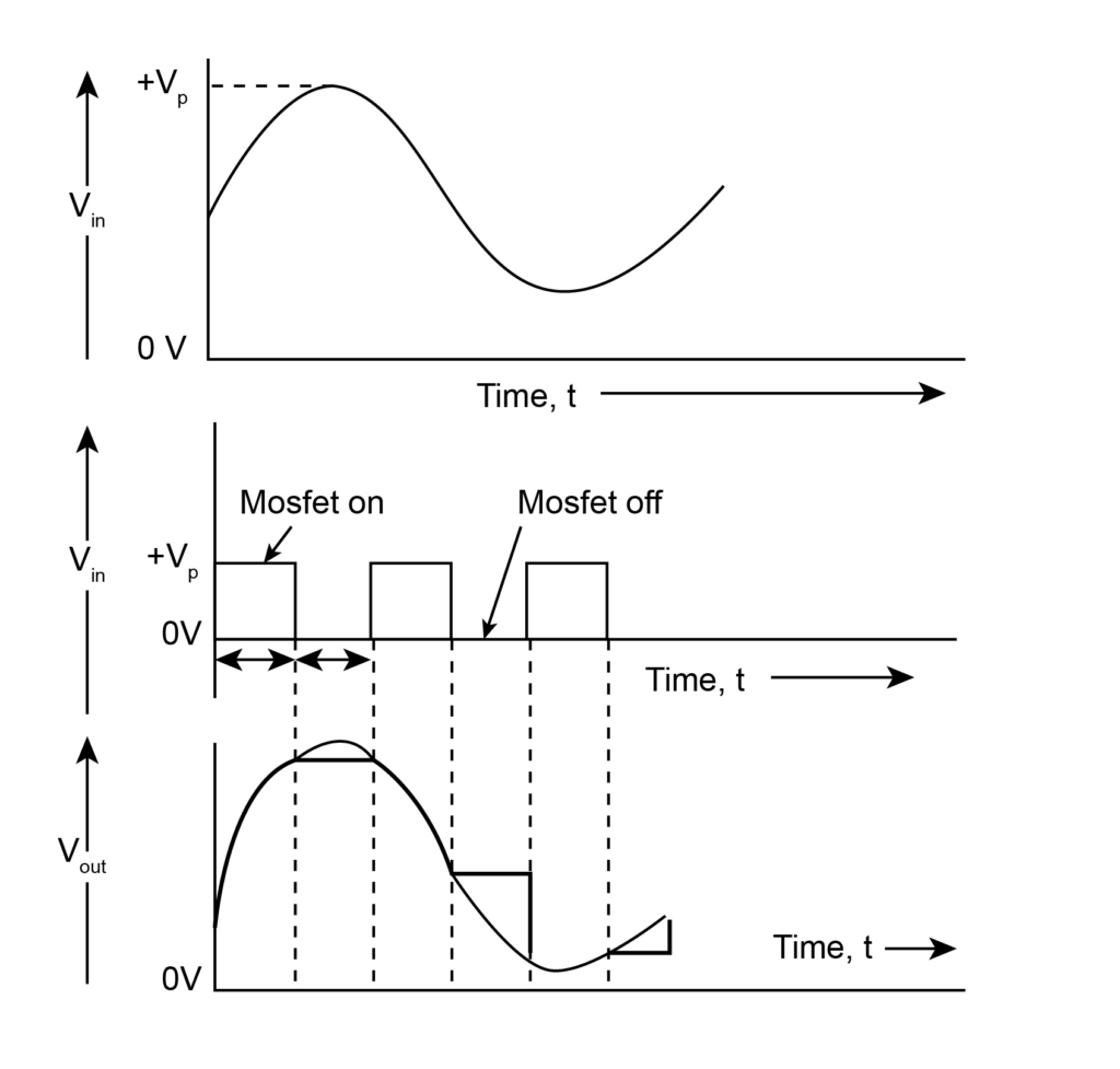
The sampling time is usually between 1 µs and 14 µs, and the capture time can take any value according to the need of the application. It would not be a mistake to say that the capacitor is the heart of the sample and the holding circuit. This is because the existing capacitor charges its maximum value when the switch is opened, that is, during the sampling period, and maintains the sampled voltage when the switch is closed.
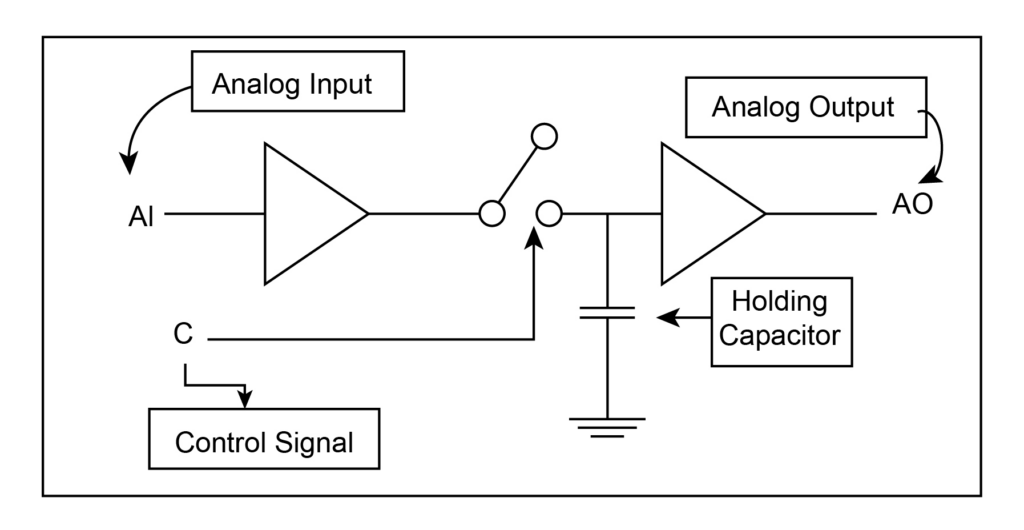
The command terminal is in logic pulse mode. Controls the input signal sample or holds the final value of the input signal sample. If the pulse is high, the signal is taken and when the pulse is low the signal is captured. The circuit, therefore, has two types of operation depending on the rational level of the Sample / Hold command signal. After receiving the input pulse command, the sample input and output sequence follow the input, that is, the output trace input, which is called the TRACK operation mode. After the command pulse is removed the integrated circuit holds the output by the value input signal it had at the time of the pulse closure; called HOLD mode.
Working principle of the sample and hold circuit
With the help of the operation of its components, it is easy to understand the operation of the sample and the maintenance of the area. The main components are sampling and circuit capture N-channel enhancement-mode MOSFETs, capacitor storage and charging power supplies, and high-performance amplifiers.
The N-channel enhancement mode MOSFET will use the switching function. The input voltage is applied to its drain terminal, and the control voltage is applied to its gate terminal. When using positive pulse, the MOSFET will switch to conduction mode. It also acts as a closed switch. Conversely, when the control power supply is zero, the MOSFET will switch to off mode and operate as an open switch.
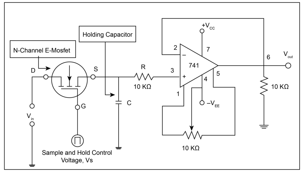
When the MOSFET is used as a closed switch, the analog signal for the discharge terminal will be supplied to the capacitor. The capacitor will then be charged to its maximum value. When the MOSFET button is turned on, the capacitor stops charging. Due to the high-performance impedance amplifier connected at the end of the circuit, the capacitor will receive high impedance and therefore cannot be discharged.
This results in delayed charging of the capacitor. This time can be called the holding time. And the time at which the input voltage samples are produced is called the sampling time. The output waveform is processed by the op-amp during holding time.
Performance Parameters of the sample and hold circuit
Acquisition Time
The capacitor determines the time required to apply the input voltage to the sample-and-hold circuit. It is called Acquisition time.
Aperture Time
The Aperture time can be defined as the time required for the capacitor to change its position from the sample to the hold. Due to the delay in the distribution of the switches, even after the catch command is given the capacitor is still charging for a short time. This is called Aperture time.
Voltage Droop
Due to the charge leakage of the capacitor, the voltage across the capacitor drops. Ideally, we need leakage capacitors, but in practice they are impossible. No matter how good quality is used, there will be a decrease in electricity.
Hold Mode Settling Time
After the capture command is generated, the analog input voltage used by the charging capacitor takes time to fully stabilize. This is called the hold mode settling time.
Need for a sample and hold circuit
Know that digital communication is advantageous compared to analog communication. However, to use the digital system, the signal used in the installation must also be in digital mode. Although initially, the signals are naturally similar. Therefore, to convert the analog signal to digital form, sample and circuit capture are used. It is usually placed before the analog to digital converter. The sample and circuit holder, the analog signal samples, and the existing capacitor hold these samples. When this sample value is provided to the ADC a signal different from the analog will be generated.
Application of the sample and hold circuit
- The biggest and most important benefit of the conventional SH circuit is to help me convert the analog conversion process to digital by capturing the analog sampled input voltage.
- Used to process analog signals.
- It can also find applications on digital voltmeters.
- During the data conversion process and in the sampling oscilloscope.
- In data distribution systems and analog-to-digital converters.
- Filters are used for signal constructional.
Common Mistakes
An important point to note here is the frequency of the analog input signal and the control signal. Maintaining good sample performance and holding the circuit is very important to maintain frequency. The frequency of the deception voltage needs to be greater than the frequency of the input voltage so that the analog signal is taken twice in the entire cycle.
Context and Applications
In each of the expert exams for undergraduate and graduate publications, this topic is huge and is mainly used for:
- Bachelor of technology in the electrical and electronic department
- Bachelor of Science in physics
- Master of Science in physics
Related Concepts
- Difference Between Analog and Digital Communication
- Oscillator
- Quantizer
- Difference Between Resistor and Capacitor
- Full-Wave Rectifiers
Practice Problems
Q1. If the interpolation characteristic is I=256, the output of the A/D converter can be obtained at a rate of 128 consecutive non-contiguous blocks.
(a) True
(b) False
Correct option: (a)
Explanation: If the interpolation characteristic is I=256, the output of the A/D converter can be obtained at the rate of 128 consecutive non-contiguous blocks. This measure may cause the value of the digital signal to range from 0 to 256 (B is 8 bits) in the Nyquist value. The averaging process also provides the necessary anti-aliasing filtering.
Q2. In DM, raising Δ reduces the distortion of the load but increases the granular noise, and vice versa.
(a) true
(b) false
Correct option: (b)
Explanation: Particular noise occurs when the DM tracks a low (slightly changing) input signal. We note that the increase in Δ reduces the distortion of multiple loads but increases the granular noise, and vice versa.
Q3. sound power can be reduced by increasing the sample volume to distribute quantization noise power over a large frequency band .
(a) true
(b) false
Correct option: (a)
Explanation: sound power can be reduced by increasing the sample volume to distribute quantization sound power over a large frequency band , and then by adjusting the spectral noise density through the appropriate filter.
Q4. What is the sampling process on the ground called?
(a) Fornication
(b) Decimation
(c) Both
(d) None of the mentioned
Correct option: (b)
Explanation: To avoid naming, we first filter out the sound outside the band (fl, F J 2) by processing the wideband signal. The signal is then transferred to a ground filter and re-sampled (low sample) at a lower cost. The lower sample process is called decimation.
Q5. What is the main function of DAC converter?
(a) Converts Digital to Analog Signal
(b) Converts Analog to Digital signal
(c) All of the mentioned
(d) None of the mentioned
Correct option: (a)
Explanation: A digital-to-analog converter (DAC) captures digital sequences and produces output current or equivalent current and digital name size used in its input.
Want more help with your electrical engineering homework?
*Response times may vary by subject and question complexity. Median response time is 34 minutes for paid subscribers and may be longer for promotional offers.
Search. Solve. Succeed!
Study smarter access to millions of step-by step textbook solutions, our Q&A library, and AI powered Math Solver. Plus, you get 30 questions to ask an expert each month.
Sample and Hold circuit Homework Questions from Fellow Students
Browse our recently answered Sample and Hold circuit homework questions.
Search. Solve. Succeed!
Study smarter access to millions of step-by step textbook solutions, our Q&A library, and AI powered Math Solver. Plus, you get 30 questions to ask an expert each month.