
Videos
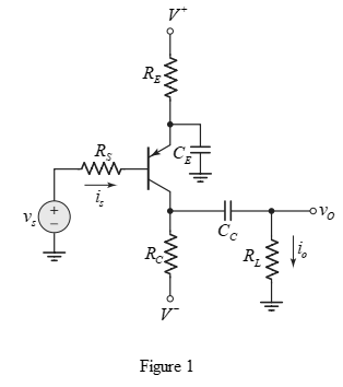
Consider the circuit shown in Figure P6.19 where the signal−source is
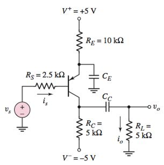
Figure P6.19
(a)
The small signal voltage gain
Answer to Problem 6.19P
The small signal voltage gain
Explanation of Solution
Given:
The sinusoidal source voltage
The circuit for
The current gain
The circuit parameters are shown below.
Concept used:
The expression for small signal voltage gain
The expression for transconductance is written below.
Calculation:
Apply dc analysis and KVL in base emitter
Substitute
The quiescent collector current is calculated as,
The transconductance is calculated as,
The diffusion resistance is calculated as,
Substitute
Therefore, the small signal voltage gain
The output current
Substitute
Therefore, the transconductance function
The output current is calculated as,
Therefore, the output current
The output voltage is calculated as,
Substitute
Therefore, the output voltage
Conclusion:
Thus, the small signal voltage gain
(b)
The small signal voltage gain
Answer to Problem 6.19P
The small signal voltage gain
Explanation of Solution
Given:
The current gain
Calculation:
Apply dc analysis and KVL in base emitter
Substitute
The quiescent collector current is calculated as,
The transconductance is calculated as,
The diffusion resistance is calculated as,
Substitute
Therefore, the small signal voltage gain
The output current
Substitute
Therefore, the transconductance function
The output current is calculated as,
Therefore, the output current
The output voltage is calculated as,
Substitute
Therefore, the output voltage
Conclusion:
Thus, the small signal voltage gain
Want to see more full solutions like this?
Chapter 6 Solutions
MICROELECT. CIRCUIT ANALYSIS&DESIGN (LL)


- 6.23 Consider the Sallen-Key lowpass circuit with the following choice made for the de- sign of the fixed elements: K = 2, R₁C₁ = R₂C₂, C₁ = 1 Determine design equations which express the values of R₁, R₂, and C₂ in terms of wo and Q.arrow_forwardAssignment-1 Q1. The output characteristic of a typical transistor is shown below, where the quiescent point is selected on it. This transistor is used in the bias circuit presented below. Find the suitable values of Rg and Rc to fix the Q-point of the circuit properly. +Vcc = 12 V 12- Ia = 70 uA 10- Is 60 uA Ta=50 A 8- Rc 6. la= 40 uA 4. Is = 30 uA 2- Is = 20 uA B = 100 VBE = 0.7 V -2- 6 8 10 12 14 16 VCE (V) toarrow_forwardQ6: a) Draw circuit (window detector) to achieve output (high) between 3V and 5.5 V if Vcc = 10V. b) Draw and explain the principle of work for 555 timer analog- digital integrated circuit converter. Then sketch the capacitor voltage and output waveforms for time high is 75% from the total periodic a 555 timer triggered by a 5-kHz. Find RA, RB. Cand Vcc = 12 Varrow_forward
- For the circuit given below, suppose that RE = 6.8k2, Rc = 4.7k2, V1 = +6V and V2 = -10V. a) Plot the small signal model and calculate the parameter of re b) Find the parameters of Zi, Zo, A, and A; Vi V2 - RE RC Iout lin HE Vout Vin Zi hfb=-1 Zoarrow_forwardHello! Please show all work, and please show verification for the triodes mode as explained at the bottom, thank you in advance :)arrow_forwardBlock Diagram: clipper R Vo V81 V82 Fig. (7) [9] Fig. (6) [8] Block Diagram: clamper Vi 10V Fig. (9) [9] Fig. (8) [9] - Describe the electronic behavior for clipper and clamper circuits. - Draw the transfer characteristic Vo versus V. toarrow_forward
- Derive the transfer function of the system shown in figure c. Page 2 of 3 R Figure (e)arrow_forwardQ6: a) Draw circuit (window detector) to achieve output (high) between 3V and 5.5 V if Vcc = 10V. b) Draw and explain the principle of work for 555 timer analog- digital integrated circuit converter. Then sketch the capacitor voltage and output waveforms for time high is 75% from the total periodic a 555 timer triggered by a 5-kHz. Find RA, RB, C and Vcc = 12 Varrow_forward1. Draw the AC equivalent circuit of the voltage divider bias configuration below with emitter bypass capacitor and determine the following parameters: a. Input impedance b. Output impedance c. Voltage gain in decibels d. Power gain in decibels 16 V 90 k C2 B= 210, r = 50 kn 76 10 0.68 k2 2. Repeat number 1 when emitter bypass capacitor is not connected.arrow_forward
- For a Step-down chopper, design the circuit with 200ohm effective input resistance and 10ohm output resistance? Calculate the duty cycle and efficiency. Assume the input voltage accordingly.arrow_forwardQ1/ Design a MOD-3, Asynchronous counter to count the following sequence: 0, 3, 6.arrow_forwardFor the circuit shown in the figure below, find the output impedance. Assume VÀ < ⁰. Vcc RE Vin KQ₁ - Vout Select one: Rc 7,₁9₂ a. rol // [Rc+ (1/9m2 // roz)] Ob. None of these Oc. ro1 [1+9m1(RE//m1)] // [Rc + (1/9m2 // m2)] O d. rol (1+9m1R) // Rcarrow_forward
 Introductory Circuit Analysis (13th Edition)Electrical EngineeringISBN:9780133923605Author:Robert L. BoylestadPublisher:PEARSON
 Delmar's Standard Textbook Of ElectricityElectrical EngineeringISBN:9781337900348Author:Stephen L. HermanPublisher:Cengage Learning
 Programmable Logic ControllersElectrical EngineeringISBN:9780073373843Author:Frank D. PetruzellaPublisher:McGraw-Hill Education
 Fundamentals of Electric CircuitsElectrical EngineeringISBN:9780078028229Author:Charles K Alexander, Matthew SadikuPublisher:McGraw-Hill Education
 Electric Circuits. (11th Edition)Electrical EngineeringISBN:9780134746968Author:James W. Nilsson, Susan RiedelPublisher:PEARSON
 Engineering ElectromagneticsElectrical EngineeringISBN:9780078028151Author:Hayt, William H. (william Hart), Jr, BUCK, John A.Publisher:Mcgraw-hill Education,