
Videos
The emitter−follower circuit shown in Figure P5.89 is biased at
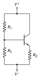
Figure P5.89
The design parameters of the circuit.
To select: Five percent tolerance values of resistances.
To find: The range of the Q- point values.
Answer to Problem D5.89DP
The design parameters of the circuit are:
Five percent tolerance resistance
The range of the current is
Explanation of Solution
Given:
The given circuit is shown in Figure 1
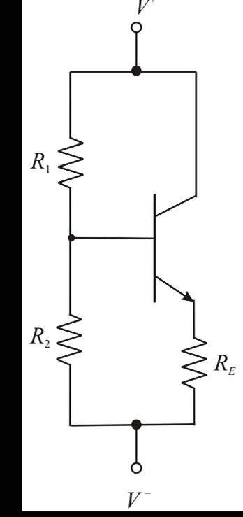
Figure 1
Calculation:
Mark the current as well as other parameters and then redraw the circuit.
The required diagram is shown in Figure 2
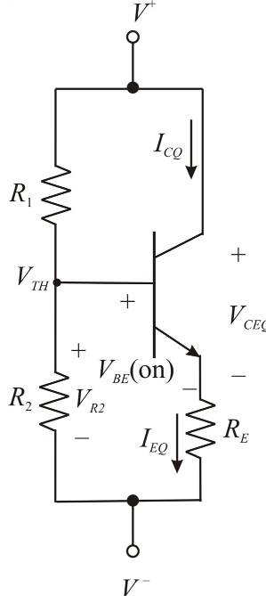
Figure 2
The Thevenin equivalent bias circuit is shown in Figure 3
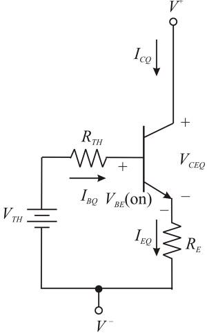
Figure 3
The value of the base current is calculated as,
Substitute
Apply KVL in Figure 2
The expression for the value of the Thevenin resistance is given by,
Substitute
Apply KVL to figure 3.
Substitute
The expression for the Thevenin voltage is evaluated as,
Substitute
The expression for the Thevenin resistance is given by,
From the five percent tolerance resistance
Now consider the value of
The value for the Thevenin resistance is calculated as,
Substitute
Substitute
The expression for the collector current is given by,
Substitute
Apply KVL in Figure 2
Consider the value of
The value for the Thevenin resistance is calculated as,
Substitute
Substitute
The expression for the collector current is given by,
Substitute
Apply KVL in Figure 2
The Q- point values of the current and voltage for the range of
Want to see more full solutions like this?
Chapter 5 Solutions
MICROELECT. CIRCUIT ANALYSIS&DESIGN (LL)


- 04:- Design a bias circuit for NPN silicon transistor having a nominal B-100 to be used in voltage divider circuit with Q-point of Ic 10 mA and VCE = 10 V. Use standard valued 5% resistors and draw a schematic diagram of your design. (10 points)arrow_forwardDraw, Illustrate and label your schematic diagram before solving the problem. 3) Given an Emitter-Stabilize Biased transistor circuit with beta DC is 250,Base resistor is 150 ohms, collector resistor is 1.5k ohms ,emitter resistor is 500 ohms ,emitter voltage supply is -5v and Voltage at common collector is +28V,Voltage at Base-emitter junction is 0.7v,. Determine Base current, Collector current and Voltage at collector-emitter junction.arrow_forwardFor the circuit given in figure below draw the collector characteristic curves for IB = 50,150 and 250 micro amperes on the same grapharrow_forward
- Pictorially describe the fabrication steps of N-channel E MOSFET. The drawing and steps be in more detailsarrow_forward1- a. For the circuits given below calculate the currents through the zener diode (V5.1V) and the current through the Si-diode. 1k Ohm 1k Ohm -10V 1k Ohm 12V b. The emitter of an NPN type BJT is connected to ground. Its base is connected to a 5V supply with a 10K resistor. Its collector is connected to the same supply with a 6K resistor. Calculate the range of ß such that the transistor is not saturated.arrow_forward- Explain the effect of base resistance and collector resistance on the circuit.arrow_forward
- A Bipolar junction Transistor with curreat amplification factor being 100, Input Base current is 50μA. Collector voltage is 10 V and biasing voltage being +20 V. Find followings a. Collector current b. Resistance (R1) c. Collector voltage , Emitter voltage , Base Voltage & Collector-Emitter Voltage.arrow_forwardAll field-effect transistors are unipolar rather than bipolar devices. That is, the main current through them is comprised either of through an N-type semiconductor * ..... .....arrow_forwardDesign the circuit below to obtain a de emitter current Ie=1.2 mA, using a power supply Vcc = 12V. The design assumes a very large B value first. After determining all resistor values, recalculate Ig for B=110. (Hint: As a rule of thumb, use VCE=- Vcc and IcRc=-Vcc and the voltage-divider current is 0.1IE). Vc Ans. R1 R, Rc R2 = Rc = RE R, R IE (B=110)=arrow_forward
- Qa: A transistor dissipates 50W in an ambient temperature of 60°C, the thermal resistances are 0-0.5 °CW¹, 8ca-4 °CW. Determine the junction temperature without a heat sink. Determine the thermal resistance of the heat sink to avoid the junction temperature exceeding 180°C. )arrow_forwardProblem5: For the common base circurt shown in figure find I. and VCB. Assume transistor is Silicon (a-0.98) Ic Rp= 1.5 ko Rc= 1.2 kn VEE = 8 V. Vcc= 18 Varrow_forwardWhat sets an integrated circuit distinct from a transistor, and what are their similarities?arrow_forward
 Introductory Circuit Analysis (13th Edition)Electrical EngineeringISBN:9780133923605Author:Robert L. BoylestadPublisher:PEARSON
 Delmar's Standard Textbook Of ElectricityElectrical EngineeringISBN:9781337900348Author:Stephen L. HermanPublisher:Cengage Learning
 Programmable Logic ControllersElectrical EngineeringISBN:9780073373843Author:Frank D. PetruzellaPublisher:McGraw-Hill Education
 Fundamentals of Electric CircuitsElectrical EngineeringISBN:9780078028229Author:Charles K Alexander, Matthew SadikuPublisher:McGraw-Hill Education
 Electric Circuits. (11th Edition)Electrical EngineeringISBN:9780134746968Author:James W. Nilsson, Susan RiedelPublisher:PEARSON
 Engineering ElectromagneticsElectrical EngineeringISBN:9780078028151Author:Hayt, William H. (william Hart), Jr, BUCK, John A.Publisher:Mcgraw-hill Education,