
Concept explainers
Videos
A.
Worst case output voltages
A.
Answer to Problem D14.47P
Worst case output voltages are
Explanation of Solution
Given:
The given circuit is:
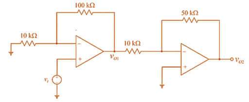
As
For first op-amp
Also
Now, KCL at input node
For second op-amp
Also
Now, KCL at input node
B.
To design:
Input bias current compensation circuit.
B.
Explanation of Solution
Given:
A simple compensation circuit can minimize the effect of bias currents in op-amp.
Consider the sketch ofinput bias current compensation circuit as,
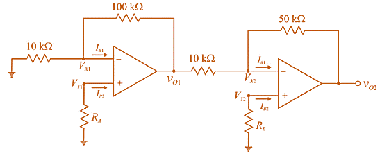
Now, determine
For first op-amp:
KCL at non-inverting node,
As,
Therefore,
KCL at inverting node,
Putting
Now,
If
For second op-amp:
KCL at non-inverting node,
As,
Therefore,
KCL at inverting node,
Putting
Now,
If
Want to see more full solutions like this?
Chapter 14 Solutions
MICROELECT. CIRCUIT ANALYSIS&DESIGN (LL)


- In Steady-State Operation o f Buck DC-DC Converter Explain how the switching frequency component is eliminated by the output filter network.arrow_forwardWrite the loop equations for a Buck converter in the two modes if the inductance is characterized by a combination of inductance L1 in series with an equivalent resistance r1, filter capacitance is characterized by a capacitor C1 in series with resistance r2. Also assume that the controlled switch has a drop of 0.4V and the freewheeling diode has a voltage drop of 0.65v. Draw the corresponding equivalent circuits in each mode.arrow_forwardQ 1. Determine the output voltage of the Digital-to-Analog Converter (DAC) in Figure 1(a) and plot it in Figure 1(c). The sequence of the four digit binary codes represented by the waveforms in Figure 1(b) are applied to the inputs. A high level is a binary 1and a low level is a binary 0. The least significant binary digit is Do. Do o D₁ 0- 200 ΚΩ www D₂ 0 100 ΚΩ www 50 ΚΩ www 25 ΚΩ D3 0 M 0 -0.25 -0.50 -0.75 -1.00 -1.25 -1.50 -1.75 -2.00 -2.25 -2.50 -2.75 -3.00 -3.25 -3.50 -3.75 (a) Vout (V) R₁ 10 ΚΩ o Vout +5 V Do 0 +5 V D₁ 0 +5 V 0 +5 V 0 D₂ D3 0 1 2 3 4 5 6 7 8 9 10 11 12 13 14 15 non (c) Figure 1 I 0000 0001 0010 0011 0100 0101 0110 0111 1000 1001 1010 1011 1100 1101 1110 1111 ||||| (b) Binary inputarrow_forward
- Positive Clamper: The function of the 2 points positive clamper is to raise the input signal to upward direction such that negative peaks falls to ..'arrow_forwardYou are tasked to look for a converter circuit design that has the specifications tabulated in Table I. The aim is to produce an output voltage of 20 V which can be used to drive a load of 120 W. The converter must operate in CCM. Table I: Design Specifications Values 35 V Design Parameters Input voltage Switching frequency Output current ripple Output voltage ripple 60 kHz 5 % 1 % a) Sketch the final converter and label all parameter valuesarrow_forward• Design a classical rectifier to deliver 100W into a resistive load from a 120V, 60HZ mains. ac Quantify the effect for different values of filter capacitance on: >average output voltage >output voltage ripple >Input current shape, harmonic content and THDarrow_forward
- The input voltage for an Op-Amp series regulator is 12v,, if the non inverting input of the op-Amp is connected to 3 series diodes instead of Zener one . a) Design the the op-amp feedback resistors to give 6.5V fixed o/p voltage b) Determine the line regulation in both % and in %/V. if the input voltage increased by 3V leading to o/p voltage increase of 0.05arrow_forwardQ2 In the circuit as shown below. Determine the (ripple factor) and sketch vp(out) for the filtered bridge rectifier with a load as indicated. 2 : 1 D3 D1 120Vp-p f= 50HZ + Output V1 V2 D2 D4 1uf R1=2karrow_forward8- Auto transformer is used in tuned amplifier to (transform low impedance of transistor input, match to the load, tune to operating frequency, stabilize tuned amplifier). 9- The dual slope A/D converter is popular because it is (fast converter, low power, low complexity, high resolution). 10- The most important feature of flash type A/D converter is (high resolution, fast, low component spread, low power dissipation).arrow_forward
- A clamping circuit has to have an independent source, a diode, a resistor, and a capacitor. To keep a constant voltage on the capacitor over the period of the input, the RC time constant must be large. A design rule of thumb is to make the RC time constant at least five times the half period of the input signal. Why do we need to make the RC time constant at least five times the half period of the input signal greater? Is having a 2, 3, or 4 times RC time constant, not enough?arrow_forwardlp ET v aph S Normal No Spacing Heading 1 Heading 2 Styles Ti The nominal output voltage of a certain regulator is 8 V. The output changes by 2 mV when the input voltage rises from 12v to 18V. Complete the following: a. Determine the line regulation and express it as a percentage change. b. Express the line regulation in %/V.arrow_forwardA signal generator having a source resistance of 50 2 is set to generate a 1 kHz sinewave. Open circuit terminal voltage is 10 V peak-to-peak. Connecting a capacitor. across the terminals reduces the voltage to 8 V peak-to-peak. The value of this capacitor is -HF. (Round off to 2 decimal places).arrow_forward
 Introductory Circuit Analysis (13th Edition)Electrical EngineeringISBN:9780133923605Author:Robert L. BoylestadPublisher:PEARSON
 Delmar's Standard Textbook Of ElectricityElectrical EngineeringISBN:9781337900348Author:Stephen L. HermanPublisher:Cengage Learning
 Programmable Logic ControllersElectrical EngineeringISBN:9780073373843Author:Frank D. PetruzellaPublisher:McGraw-Hill Education
 Fundamentals of Electric CircuitsElectrical EngineeringISBN:9780078028229Author:Charles K Alexander, Matthew SadikuPublisher:McGraw-Hill Education
 Electric Circuits. (11th Edition)Electrical EngineeringISBN:9780134746968Author:James W. Nilsson, Susan RiedelPublisher:PEARSON
 Engineering ElectromagneticsElectrical EngineeringISBN:9780078028151Author:Hayt, William H. (william Hart), Jr, BUCK, John A.Publisher:Mcgraw-hill Education,