Rc2 RCi oF Qc oY A VREF Op QE RB RE VEE
Q: 3) a) What is the logic function that is implemented by the gate in the below figure? b) What are…
A:
Q: 4. In the logic circuit shown below, what is the minimum RL that the inverter drive without causing…
A:
Q: 4. In the logic circuit shown below, what is the minimum RL that the inverter can drive without…
A:
Q: 3) (a) Find VH, VL , and the power dissipation (for vo = Vz ) for the logic inverter with resistor…
A: It is given that: Kn'=100 MAV2Kp'=40 MAV2VTN=0.6 VVrp=0.6 V
Q: Given the logic expression: Y=A+BC+ABD+ABC 1-Express it in standard SOP form 2-Draw K-map and…
A: Given logical expression, Y=A+B¯ C¯+ABD¯+ABCD. Some Boolean properties are mentioned below which can…
Q: 3) Consider the CMOS logic gate that implements the function Y = C + BD + CBA a) Draw the circuit…
A: Given: The CMOS logic gate that implements the function: Y=C+BD+C¯BA To find: a) Draw the circuit…
Q: The logic swing in the inverter as shown is reducedby a factor of 3 by reducing the value of RCand…
A: Calculating collector resistance RC’ Calculating logic swing voltage
Q: A logic gate has two inputs A and B. Its output is equal to a 1 if and only if the two inputs A and…
A: Given a logic gate whose output will be 1 when both inputs are same.
Q: For a CMOS logic gate circuit given below a.) Sketch and Label the types of MOSFET for MI, M2, M3,…
A:
Q: Speed Power Product (SPP) is a figure of merit of a logic circuit which is based on the product of…
A: speed power product = propagation delay(ns)* power dissipation(mW) power dissipation = voltage *…
Q: 8.2. Draw the equivalent Logic Gate Circuit of the Ladder Circuit below. Out1 H
A: The functioning of a digital logic circuit is defined by a collection of laws and rules called…
Q: ) (a) Find VH , V1 , and the power dissipation (for vo = V1 ) for the logic inverter with resistor…
A: Resistors are coupled to an inverter's DC bus circuit, consume motor regeneration power, and…
Q: Convert the BCD to Excess-3 converter to its NOR gate equivalent form. Draw the logic diagram (Not…
A:
Q: 5. For the figure below, with a CLK buffer delay of 2.0 ns, other buffer delays of 1.5 ns,…
A: Setup time is the time duration for which the data should be stable before the clock edge arrival.…
Q: For a CMOS logic gate circuit given below a.) Sketch and Label the types of MOSFET for Ml, M2, M3,…
A: According to the bartleby's guidelines we have to solve only first three subparts of a question so…
Q: Find VH for an NMOS logic gate with a saturatedload if VT O = 0.75 V, γ = 0.75 √V, 2φF = 0.7 V,and…
A: Given data: VTO is: 0.75 V VDD is: 3.0 V The expression for the VH is given as, The expression for…
Q: Figure Q.4(a) shows a JK Nip-flop with active-LOW preset (PRE) and clear (CLR) functions. PRE CLK…
A: In digital circuits, flip-flops (FF) are used to store one-bit information. Based on the inputs and…
Q: 1- Implement ( without simplification) F= (A+B).(C+A.D) using NAND gates only. 2. Desion a logic…
A: As per Bartleby guidelines we are allowed to solve only one question, please ask the rest again.
Q: Problem 2. The following diagram shows a schematic for the pullup circuitry for a particular CMOS…
A: (A) the schematic for the pulldown circuitry for this CMOS gate is shown below,
Q: Q1 Write the difference between TTL and CMOS logic families according to the following table:…
A: The difference between TTL and CMOS according to the given parameter is shown in table. The power…
Q: Design a gate-level implementation for the following expressions using the specified gate types. Use…
A: NAND AND NOR NAND and NOR are called universal gates because any logic functions can be…
Q: 6. Show that the circuit shown below functions as a logic inverter VDD Qi Vout Vin Q2
A: The explanation can be achieved as follow.
Q: 2) Find VH, VL, and power dissipation (for vo = V1) for the logic inverter with saturated load in…
A:
Q: Q4: Given the table below that shows the tcp and tpp for each of the logic gate in the circuit…
A:
Q: For the logic function in the figure below fill in the NMOS transistors and with a 1.0V supply…
A: We have given the following problem
Q: Convert the logic diagram below to both NAND and NOR implementations. B D 거 E
A: Given here a Logic diagram and asked to implement it with NAND and NOR Gates.
Q: For the transistor in this question, assume Vpp= 1.8V, µCox= 600µAV1, HpCox= 200µAV*1, Vthl= 0.5 V,…
A: Given, VDD= 1.8V, UnCox= 600 microAV-1 , Vth=0.5v and UpCox= 200 microAV-1
Q: In the logic circuit shown below, what is the minimum RL that the inverter can drive without causing…
A: Given Vi = 0 V V0 = 4 V Vcc = 5 V Rc = 100
Q: a) Design (Find the values of W/L for NMOS and PMOS) a reference CMOS inverter to achieve a delay of…
A:
Q: Identify the correct statement with respect to CMOS logic family O a. High power dissipation O b.…
A: In CMOS logic family,
Q: Find VH for an NMOS logic gate with a saturatedload if VT O = 0.6 V, γ = 0.6√V, 2φF = 0.6 V,and VDD…
A: Given data: VTO=0.6 Vγ=0.6VVDD=3.3 V The expression for the VH is given as, VH=VDD-VTNL The…
Q: Q1: A/ Design and draw a logic circuit that compares between two 3-bit binary numbers. The circuit…
A: MAGNITUDE COMPARATOR: This circuit is used to compare two binary numbers but only their magnitude is…
Q: 4) Find VH, VL, and power dissipation (for vo= V1) for the logic inverter with linear load inverter…
A:
Q: Provide the correct answer and write a legible solution. 1. Simplify the expression G = (X’ + Y +…
A:
Q: Q10 (a) State in words and in the form of a truth table the actions of the following logic gates.…
A: AND GATE : Statement : Whenever both the inputs are logic high then only output is logic for any…
Q: Design a logic cirčuit with four inputs and if the input patterns have odd number of zeros. a) Write…
A:
Q: CMOS with a PDP of 50 fJ is to be used in a chipdesign that requires 100 million gates. The chip…
A: Given: To find the minimum logic gate delay that can be used in the design if all the gates operate…
Q: Due to availability of NAND gate ICs only, design a digital logic circuit for the following…
A:
Q: Provide the correct answer and write a legible solution. 1. Simplify the expression F = ABCD + AB’CD…
A: According to the question we have to find the value of simplified given expression and draw logic…
Q: Implement the following logic function using complementary CMOS. a) Y = ((Ā + B) ·(Č +D+ E) + F) · G…
A:
Q: Consider a dynamic domino logic circuit shown below. Suppose that each transistor has an internal…
A: Given : WN1 = WN2 = WN3 =1 u WP1 =2 u WP-1n =2u WN-1n=1 u L= 1 u Solution(a) The powee absorbed by…
Q: a) A standard TTL inverter gate is shown in the figure. The supply voltage is 5V. Calculate the…
A: Solution (a) - When Vi =0.1 V Thus, when the input voltage is 0.1 V than output voltage is 4.28 V.
Q: Draw the transistor schematic for the logic gate corresponding to the Euler paths above. Make sure…
A: CMOS is a gate which is consist of nMOS (Pull up network) and pMOS (pull down network).
Q: Assume Vth = 1V and k = 50mA/V2. Given the schematic below, do the following: 1) Indicate and…
A: 1)
Q: Figure 1 shows a 2-input TTL NAND gate. Discuss in details the operation of the NAND circuit Is this…
A: TRUTH TABLE OF TWO INPUT NAND :- 1) A B Z…
Q: 4) Design a saturated-load gate that implements the logic function Y = A(B +C D) + E . base on the…
A: Logic gates- Logic gates are mathematical exponential process deals with true or false values…
Q: Simplify the expression G = (X’ + Y + Z’) (W + X + Y + Z) (W’ + X’ + Y’) using K- map and draw the…
A:
Assume that you need 0.6 V across RE to properly
stabilize the current in the modified ECL gate
as shown. Design the resistors in the gate for
a logic swing of 0.4 V and an average current of
1 mA through RB and RE . What are the minimum
values of VEE and the value of VREF?
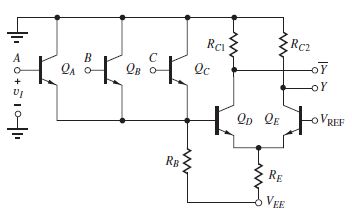
Step by step
Solved in 5 steps with 9 images
- FAIRCHILD Discrete POWER & Signal Technologies SEMICONDUCTOR ru 1N4001 - 1N4007 Features • Low torward voltage drop. 10 a14 * High aurge eurrent cepablity. 0.160 4.06) DO 41 COLOR BAND DGNOTEs CAT-Cos 1.0 Ampere General Purpose Rectifiers Absolute Maximum Ratings T-26*Cuness atnerwioe rated Symbol Parameter Value Units Average Recttied Current 1.0 375" lead length a TA - 75°C Tsargei Peak Forward Surge Current 8.3 ms single halr-sine-wave Superimposed on rated load JEDEC method) 30 A Pa Total Device Dissipetion 2.5 20 Derste above 25°C Ra Tag Thermal Resistence, Junction to Amblent 5D Storage Temperature Range 55 to +175 -55 to +150 Operating Junetion Temperature PC "These rarings are imithg valuee above whien the serviceatity or any semiconductor device may te impaired. Electrical Characteristics T-20'Cunieas ofherwise roted Parameter Device Units 4001 4002 4003 4004 4005 4006 4007 Peak Repetitive Reverse Vellage Maximum RME votage DC Reverse Voltage Maximum Reverse Current @ rated VR…Hw@: : A555 IC is Connected 95 slhown in fingune below; fingune Detarmine the range of oscillation finaguerney? Ans: VCC =1Ov 1ok trag. range (621H2 -4.7 kllz 4 7. loke 555 IC 2. CPotentiometa10oke D.olHFCircuit plz helppppppp
- Repeat example 35 for FWD and firing angle Fa) 60°. 215 l65 D1985 Example 35: A full wave rectifier used 220V, with firing angle 10° ,total resistance load 5 KQ, inductance 2.34 H,and frequency 60HZ, Draw and calculate: (a) VD.c and Ipc (b) VD.C(Max) (c) Vn (d) Vorms-Determine the approximate value *3. Graphical Representation of the signal 1) Write the type of the voltage from simulation results: 2) Write the value of the voltage from simulation result: L....... -2 DDU 12ns SónG Trace Color Trace Name X Values CURSOR 1,2 V(R1:1,0) Y1 Y2 Y1 - Y2 5.0373m 0.000 5.0373m 249.983 0.000 249.983 Y1(Cursor1) - Y2(Cursor2) Y1-Y1(Cursor1) Y2 - Y2(Cursor2) Max Y Min Y Avg Y 249.983 0.000 0.000 249.983 0.000 124.991
- I want to design an oscillator for a PWM supply. It will run with a square wave of 75 KHz. Voltage is 15VDuty Cycle about 50%. Hint: Choose values of resistor, and then calculate capacitor for the frequency. Draw the circuit. Show the calculations.Give the meaning of each acronym of solid state devices. Also sketch the schematic symbol for each device. SUS Shockley diode D-MOSFET JFET SCR DIAC THYRISTOR Device TRIAC 1. 3. 4. 6. 8. 10. 12. 14. Symbol 2. 5. 7. 9. 11. 13. 15. Meaning No entryA. Find the value of Ibq B. Find the value of Rf C. Find the value of (Re) t
- Please answer all subpart please sir ASAP for like this..Digital Circuits QuestionLTE .!!: 0:00 docs.google.com a What will be the out put of the D'Arsonval meters, if an average responding a.c meter of half-wave rectifier read (2.36 v), and true form factor of input waveform is (1.414). 3 volt 1.5 volt 1 volt 2.36 volt If the value of waveform does not remain constant with time, the signal is referred to as direct (d.c) signal * True False •.. 6 +