
Introductory Circuit Analysis (13th Edition)
13th Edition
ISBN: 9780133923605
Author: Robert L. Boylestad
Publisher: PEARSON
expand_more
expand_more
format_list_bulleted
Related questions
Question
Post-Lab Questions
• What are the benefits of making a Boolean equation as minimal as possible?
• Which segment required the least amount of circuitry? What makes this so?
• Describe in detail the test plan used to verify the design, as well as the debugging process used to correct any errors.

Transcribed Image Text:Seven-Segment Display
A seven-segment display (SSD) is an electronic device used for displaying numerical values. The device
typically consists of seven segments arranged in a figure 8. Any digit, as well as some alphabet letters,
can be displayed when the correct segments are activated. An example of an SSD as well as possible
outputs can be seen in Figure 3.
889
Figure 3 - Seven-Segment Display with Numeric Outputs
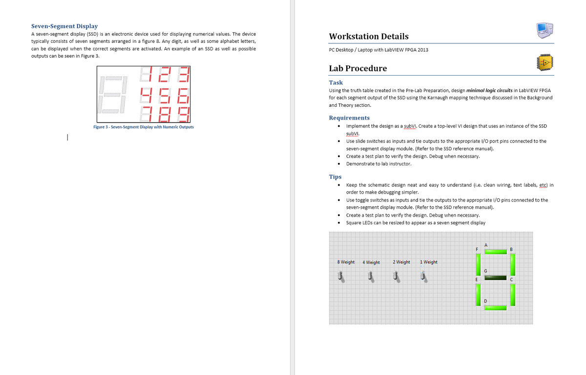
Workstation Details
PC Desktop / Laptop with LabVIEW FPGA 2013
Lab Procedure
Task
www
Using the truth table created in the Pre-Lab Preparation, design minimal logic circuits in LabVIEW FPGA
for each segment output of the SSD using the Karnaugh mapping technique discussed in the Background
and Theory section.
Requirements
•
Implement the design as a subVI. Create a top-level VI design that uses an instance of the SSD
subVI.
Use slide switches as inputs and tie outputs to the appropriate I/O port pins connected to the
seven-segment display module. (Refer to the SSD reference manual).
• Create a test plan to verify the design. Debug when necessary.
Demonstrate to lab instructor.
Tips
•
•
Keep the schematic design neat and easy to understand (i.e. clean wiring, text labels, etc) in
order to make debugging simpler.
Use toggle switches as inputs and tie the outputs to the appropriate I/O pins connected to the
seven-segment display module. (Refer to the SSD reference manual).
•
Create a test plan to verify the design. Debug when necessary.
•
Square LEDs can be resized to appear as a seven segment display
8 Weight
4 Weight
2 Weight
1 Weight
J
A
F
B
G
D

Transcribed Image Text:Lab 2 - Karnaugh Maps
Due Date: Sunday of Week 5 by 11:55 PM
In this lab experiment, the student will design a minimized, seven-segment display decoder circuit using
Karnaugh maps. This lab requires knowledge of Karnaugh map simplification which is briefly discussed
in the Background & Theory section of this lab handout.
ABCO
C
0 0 00
0
1
AB
0 0 1 1
0 1 0 0
00
0
1
0 1 1 0
01
0
0
1 0 0 1
1 0 1 1
11
1
0
1 1 0 1
10
1
1
1 1 1 0
Objectives
Create minimal logic circuits using Karnaugh map simplification.
✓ Design a minimal seven-segment display decoder.
Simulate the circuit in LabVIEW
Pre-Lab Preparation
For this lab, you will design digital hardware to interface with a seven-segment display module. Read the
following manual and note the layout of the segments as well as their assigned pins:
http://www.opled.com.tw/ShowProductPDF.aspx?p_id=811
Create a truth table with inputs for a 4-bit binary number and outputs for each of the seven-segments of
the display. Fill the output values so the segments will be lit to represent the decimal value of binary
input. For example, the row with the binary input equal to 0111 should have a corresponding output
row with the A, B, and C segments set to 1 to indicate a decimal value of 7 on the display. Since you are
only concerned with single digit decimal values (0-9), mark the remaining unused rows as Don't Cares.
Figure 1 - Karnaugh Map Representation of Truth Table
After transferring the truth table to a Karnaugh map, cells with common output values, either all Os or
all 1s, are grouped into the largest possible rectangles such that the number of cells in the groups is
equal to 2² and i is some integer value. Valid cell group arrangements include 4 cells in a line, 2 cells high
by 4 cells long, 2 cells by 2 cells, etc. The cells can be used more than once only if it generates the least
number of groups. Also, all cells sharing the chosen common output must be contained within a
grouping.
The groups generated can be converted to a Boolean expression. Each group represents a minimal
minterm (1s) or maxterm (Os). The term is minimized by eliminating variables whose non-inverted and
inverted forms appear within the same cell group. The terms are then used to derive an SOP or POS
expression form of the represented logic function, which may then be converted to a CLC. When
choosing the POS form, the variable combination is supposed to equal 0, as is the case when deriving a
POS from a truth table. Therefore, the variable's inverse is used when determining a maxterm. Figure 2
illustrates a Karnaugh map translated to minimized SOP and POS expression forms. Notice how cells can
also wrap around the map.
CD
AB
00
01
11
10
Background & Theory
Karnaugh Map
A Karnaugh map is a handy tool used to derive a minimal Boolean expression from a non-simplified
form. Ultimately, the primary use of a Karnaugh map is realizing a minimal Boolean equation.
Similar to the number of rows in truth table, a Karnaugh map consists of 2" cells, where n is the number
of Boolean input variables. Each cell represents two significant aspects of a Boolean function-a variable
combination and its corresponding output value. The cells are formed in a square or rectangle fashion
and arranged such that neighboring cells have a single variable difference, otherwise known as Gray
code ordering. For simplicity, the input values are placed as column and row labels. A truth table
represented as a Karnaugh map is shown in Figure 1.
00
01
11
10
SOP (1's): AC + A'D' + B'D'
K-map Color
POS (0's): (A+D') (C+D') (A'+B'+C)
K-map Color
Figure 2 - Karnaugh Map to Minimized SOP and POS Expression Forms
Furthermore, an output state level may be a Don't Care which represents a state that is negligible,
typically because it will never occur. These cells should only be grouped if the resulting cell group is
larger than the group formed without it. In other words, only use Don't Cares if it further simplifies the
Boolean express; otherwise, ignore it.
Expert Solution
This question has been solved!
Explore an expertly crafted, step-by-step solution for a thorough understanding of key concepts.

Step by stepSolved in 2 steps

Knowledge Booster

Similar questions
- Construct MOD 12 asynchronous counter. What will be the output frequency, if the input frequency is 1 MHz. If the counter is at state 6, what will be the count after 60 pulses.arrow_forwardNeeds Complete solution with 100 % accuracy don't use chat gpt or ai plz plz plz.arrow_forward3. Sweep Vin (0 to 1V) and plot Id. Vth = 0.4V. Indicate the region of operation clearly. 1V Jid Vinarrow_forward
- Calculate the offset for the physical address 00062 H and segment address FFFFH,arrow_forwardThe error detector compares the ....to the and .. .. produces an error signal equal to the difference between the two. setpoint/desired output measured output/actual output desired output/measured output Set point/Measured outputarrow_forward(d) In a certain clock generation circuitry, the input range of the PLL is 3MHZ – 6MHZ. If the input clock is 16MHZ. what are the best values for the divider and PLL setting to get 20MHZ at the output of the clock generation circuitry?arrow_forward
- i need the answer quicklyarrow_forwardPRO3. In a point of view of voltage polarity, what is the difference between the output PWM signals in experiments 11-1 and 11-2? H ICTS Experiment 11-1.. Pulse Width Modulator Using uA741 Experiment 11-2 Pulse Width Modulator Using LM555arrow_forwardAssume a block diagram for a clock divider that can take a 1 MHz oscillator and create a signal that has clock frequency of 20 Hz. What is the terminal count value needed to create this frequency and the number of bits needed on the counter if the clock divider can select between a 20 Hz signal and 2 kHz signal?arrow_forward
- The image added shows a digital modulator. State what the modulation scheme is and show how the modulated sequence 101 looks like if one bit contains three periods of the carrier sine wave, for the following types of modulating binary sequences: a) Unipolar b) Bipolararrow_forwardFor the DBPSK modulator shown in Figure 40a (page 93), determine th output phase sequence for the following input bit sequence: 00110011010101 (assume that the reference bit 1). * 0°180°0°0°0°180°0°0°0°180°180°o°0°180°180°0°180° 10111011100110010 180°0°0°0180°0°0°0180°180°180°0°0180°180°0°0° 01110111000110011arrow_forwardAn ideal ADC has a resolution of 6 bits and a conversion voltage range between -2 V and 4 V. What is the conversion resolution? Enter a value in millivolts (mV) to 2 decimal places.arrow_forward
arrow_back_ios
SEE MORE QUESTIONS
arrow_forward_ios
Recommended textbooks for you
- Introductory Circuit Analysis (13th Edition)Electrical EngineeringISBN:9780133923605Author:Robert L. BoylestadPublisher:PEARSON
 Delmar's Standard Textbook Of ElectricityElectrical EngineeringISBN:9781337900348Author:Stephen L. HermanPublisher:Cengage Learning
 Programmable Logic ControllersElectrical EngineeringISBN:9780073373843Author:Frank D. PetruzellaPublisher:McGraw-Hill Education
  Fundamentals of Electric CircuitsElectrical EngineeringISBN:9780078028229Author:Charles K Alexander, Matthew SadikuPublisher:McGraw-Hill Education
 Electric Circuits. (11th Edition)Electrical EngineeringISBN:9780134746968Author:James W. Nilsson, Susan RiedelPublisher:PEARSON
 Engineering ElectromagneticsElectrical EngineeringISBN:9780078028151Author:Hayt, William H. (william Hart), Jr, BUCK, John A.Publisher:Mcgraw-hill Education,
Introductory Circuit Analysis (13th Edition)
Electrical Engineering
ISBN:9780133923605
Author:Robert L. Boylestad
Publisher:PEARSON
Delmar's Standard Textbook Of Electricity
Electrical Engineering
ISBN:9781337900348
Author:Stephen L. Herman
Publisher:Cengage Learning
Programmable Logic Controllers
Electrical Engineering
ISBN:9780073373843
Author:Frank D. Petruzella
Publisher:McGraw-Hill Education
Fundamentals of Electric Circuits
Electrical Engineering
ISBN:9780078028229
Author:Charles K Alexander, Matthew Sadiku
Publisher:McGraw-Hill Education
Electric Circuits. (11th Edition)
Electrical Engineering
ISBN:9780134746968
Author:James W. Nilsson, Susan Riedel
Publisher:PEARSON
Engineering Electromagnetics
Electrical Engineering
ISBN:9780078028151
Author:Hayt, William H. (william Hart), Jr, BUCK, John A.
Publisher:Mcgraw-hill Education,