
Introductory Circuit Analysis (13th Edition)
13th Edition
ISBN: 9780133923605
Author: Robert L. Boylestad
Publisher: PEARSON
expand_more
expand_more
format_list_bulleted
Related questions
Question
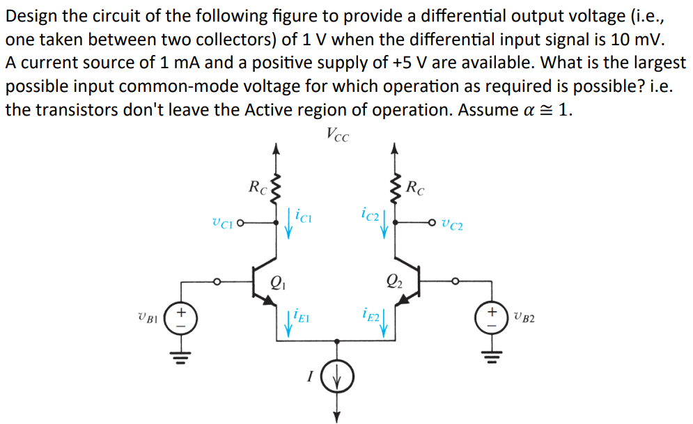
Design the circuit of the following figure to provide a differential output voltage (i.e.,
one taken between two collectors) of 1 V when the differential input signal is 10 mV.
A current source of 1 mA and a positive supply of +5 V are available. What is the largest
possible input common-mode voltage for which opera.on as required is possible? i.e.
the transistors don't leave the Active region of operation. Assume alpha ≅ 1.

Transcribed Image Text:Design the circuit of the following figure to provide a differential output voltage (i.e.,
one taken between two collectors) of 1 V when the differential input signal is 10 mV.
A current source of 1 mA and a positive supply of +5 V are available. What is the largest
possible input common-mode voltage for which operation as required is possible? i.e.
the transistors don't leave the Active region of operation. Assume a ≈ 1.
Vcc
VBI
UCIO
Rc
Rc
VC2
γει
+
UB2
I
Expert Solution
This question has been solved!
Explore an expertly crafted, step-by-step solution for a thorough understanding of key concepts.

Step by stepSolved in 2 steps with 2 images

Knowledge Booster

Similar questions
- Just need 1d and 1e answered.arrow_forwardExercise 1:-arrow_forwardcircuits by using the small signal models of the transistor. Assume the Early voltage of the transistors are infinitely large. Calculate the small-signal input and output impedances of the following Vcc R1 R1 Rout VB RE Rin R2arrow_forward
- The small-signal model is said to be valid for voltage variations of about 5 mV. To what percentage current change does this correspond? (Consider both positive and negative signals.) What is the maximum allowable voltage signal (positive or negative) if the current change is to be limited to 10%?arrow_forwardThe collector characteristics for a certain transistorare shown a. Find the ratio Ic/IB for VCE =10 V and IB =100,200, and 600 pA.b. The maximum allowable collector powerdissipation is 0.5 W for IB = 500 pA. Find VCE. Hint: A reasonable approximation for the power dissipatedat the collector is the product of the collector voltage andcurrent P = IcVCE, where P is the permissible powerdissipation, Ic is the quiescent collector current, and VCE iSthe operating point collector-emitter voltage.arrow_forwardThe DC Current Gain of a Transistor is Select one: a. Ratio of Collector Current to Base Current b. Ratio of Base Current to Collector Current c. Ratio of Emitter Current to Collector Current d. Ratio of Base Current to Emitter Currentarrow_forward
- What must be the minimum power rating for the external pass transistor used with a 7815 regulator in a circuit such as that shown in Figure below? The input voltage is 30 V and the load resistance is 10 n. The maximum internal current is to be 700 mA Assume that there is no heat sink for this calculation. Keep in mind that the use of a heat sink increases the effective power rating of the transistor and you can use a lower rated transistor. Qeu VIN Re VOUT 7815arrow_forward1. For the circuit in Figure 1: a) Calculate the input and output power if the input signal results in a base current of 5 mA rms. b) Calculate the input power dissipated by the circuit if RB is changed to 1.5 kN. c) What maximum output power can be delivered by the circuit if RB is changed to 1.5 kN? d) If the circuit is biased at its center voltage and center collector operating point, what is the input power for a maximum output power of 1.5 W? +Vcc (18 V) RC -16Ω RB 1.2 k2 B - 40 100 µFarrow_forward1. For the circuit in Figure 1: a) Calculate the input and output power if the input signal results in a base current of 5 mA ms. b) Calculate the input power đissipated by the circuit if Rs is changed to 1.5 kQ. c) What maximum output power can be delivered by the circuit if RE is changed tol.5 kQ? d) If the circuit is biased at its center voltage and center collector operating point, what is the input power for a maximum output power of 1.5 W? +Vcc (18 V) Re = 16 2 1.2 kS2 B-40 100 pF Figure 1arrow_forward
- 1. For the circuit in Figure 1: a) Calculate the input and output power if the input signal results in a base current of 5 mA rms. b) Calculate the input power dissipated by the circuit if Rg is changed to 1.5 kN. c) What maximum output power can be delivered by the circuit if RB is changed to 1.5 kN? d) If the circuit is biased at its center voltage and center collector operating point, what is the input power for a maximum output power of 1.5 W? +Vcc (18 V) Rc = 16 2 RB 1.2 k2 V. B - 40 100 µF Figure 1arrow_forwardA. For the configuration shown below in 4(A), find the small signal voltage gain (Voutp-Voutm)/Vin B. For the configuration shown in 4(B), find the following parameters (a) DC value of output voltage, (b) input common mode range and (c) small signal voltage gain when all transistors are in saturation vou/Vin as indicated in the diagram; Assume no body bias on M1 ad M2 For this problem ONLY, assume the following device parameters V7, = \V| = 0.5V;K, = k ,' = 100 µA / V²,a, = a, = 0.01 VDD = 3V (10/1) M, M. (10/1) (10/1) M, |M, (10/1) Voutp 20kΩ м, (200/1) м, м, (10/1) м, Vin (1/1) м, M. (10/1) + Vin DC VAN M, 100HA (1/1) M, M, (10/1) (A) (B) V. =-1Varrow_forwardThe amplifier in the circuit below is driven by a signal generator v, with a small sine wave signal vhose average value is zero. Assume the transistor has a value of B-100, and V-26 mV. a. You need to design the circuit so that the de emitter current IE of the emitter resistor RE to establish the desired de emitter current. = 1 mA. Specify the value b. A de collector voltage of +5 volts is desired. Specify the value of the collector resistor Re to establish the desired de collector voltage. For this part assume that RL 5 K and the Early Effect needs to be considered. The transistor has a VA 100 Volts. Draw the ac small signal equivalent circuit model of the amplifier and determine its voltage gain. 91SV C. 2.5k MM do RE -15 V 84 Vout RLarrow_forward
arrow_back_ios
SEE MORE QUESTIONS
arrow_forward_ios
Recommended textbooks for you
- Introductory Circuit Analysis (13th Edition)Electrical EngineeringISBN:9780133923605Author:Robert L. BoylestadPublisher:PEARSON
 Delmar's Standard Textbook Of ElectricityElectrical EngineeringISBN:9781337900348Author:Stephen L. HermanPublisher:Cengage Learning
 Programmable Logic ControllersElectrical EngineeringISBN:9780073373843Author:Frank D. PetruzellaPublisher:McGraw-Hill Education
  Fundamentals of Electric CircuitsElectrical EngineeringISBN:9780078028229Author:Charles K Alexander, Matthew SadikuPublisher:McGraw-Hill Education
 Electric Circuits. (11th Edition)Electrical EngineeringISBN:9780134746968Author:James W. Nilsson, Susan RiedelPublisher:PEARSON
 Engineering ElectromagneticsElectrical EngineeringISBN:9780078028151Author:Hayt, William H. (william Hart), Jr, BUCK, John A.Publisher:Mcgraw-hill Education,
Introductory Circuit Analysis (13th Edition)
Electrical Engineering
ISBN:9780133923605
Author:Robert L. Boylestad
Publisher:PEARSON
Delmar's Standard Textbook Of Electricity
Electrical Engineering
ISBN:9781337900348
Author:Stephen L. Herman
Publisher:Cengage Learning
Programmable Logic Controllers
Electrical Engineering
ISBN:9780073373843
Author:Frank D. Petruzella
Publisher:McGraw-Hill Education
Fundamentals of Electric Circuits
Electrical Engineering
ISBN:9780078028229
Author:Charles K Alexander, Matthew Sadiku
Publisher:McGraw-Hill Education
Electric Circuits. (11th Edition)
Electrical Engineering
ISBN:9780134746968
Author:James W. Nilsson, Susan Riedel
Publisher:PEARSON
Engineering Electromagnetics
Electrical Engineering
ISBN:9780078028151
Author:Hayt, William H. (william Hart), Jr, BUCK, John A.
Publisher:Mcgraw-hill Education,