
Related questions
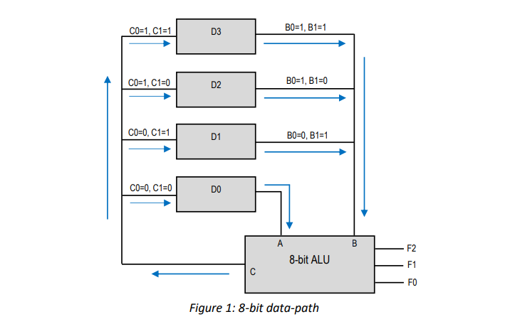
Show an image of the completed 8 BIT ALU The most important and possible most difficult component to implement is the arithmetic logic unit. The
functions of the ALU are shown in Table 1. The ALU should have 5 inputs (A-input, B-input, F0-input, F1-input, Finput) and 1 output (C-output). You will need to determine how many bits each input and output should have.
Remember, you are designing an 8-bit microprocessor! To achieve the specified ALU functions, think about
which digital logic component(s) you can use to accomplish the task. For example, to add the value on the A-bus
8-bit ALU
to the value on the B-bus, you can simply use an 8-bit adder. Explore the components in Logisim! Additionally,
you can think about using a multiplexer to determine which ALU function will be performed


Step by stepSolved in 1 steps


- a- Draw & explain the block diagram of synchronous sequentialcircuits.b- Design & draw a (3 × 2) binary digit multiplier, explaining itsmechanism of operation.arrow_forwardUsing Logism Softwarel The most important and possible most difficult component to implement is the 8 bit arithmetic logic unit. Thefunctions of the ALU are shown in Table 1. The ALU should have 5 inputs (A-input, B-input, F0-input, F1-input, Finput) and 1 output (C-output). You will need to determine how many bits each input and output should have.Remember, you are designing an 8-bit microprocessor! . For example, to add the value on the A-bus8-bit ALUto the value on the B-bus, you can simply use an 8-bit adder. Explore the components in Logisim! Additionally,you can think about using a multiplexer to determine which ALU function will be performedarrow_forward1. The following figure shows the four-bit Adder. Your inputs for this combinational circuit are A = 3 and B = 5. What is the outputs S3, S₂, S₁, and So? You have to show how to get the outputs by indicating each carry bit. (Note: You should show all the steps to receive full credits) CA A3 FA B3 S3 C3 A₂ B₂ FA S2 C₂ A₁ B₁ FA S₁ C1 Ao Bo FA So Coarrow_forward
- Task 5: Use NAND gates and inverters only to rebuild the circuit. a. Draw the circuit diagram below. b. Build a circuit using Multisim that is based on the above diagram and record the outputs in the columns of "Sim. O". A 0 0 1 1 B 0 1 0 1 Calculated Sim. 0₁ 0₁ Calculated 0₂ Sim. 0₂ Calculated 03 Sim. 03arrow_forwardDesign and implement (draw the circuit) the output f(12) of a 7 segments decoder as a function of the binary inputs (W,X,Y,Z). You need the complete the following steps: 1. Find the f(12) outputs values (0 or 1) for each number from 0-11 2. Enter these values into a Karnaugh map. 3. Simplify the map. 4. Draw the circuit using Tina. 7 segments display decoder. 7 segments 4 Binary inputs a 7 Segments Decoder Y earrow_forwardSolve number 2arrow_forward
- Computer Networking: A Top-Down Approach (7th Edi...Computer EngineeringISBN:9780133594140Author:James Kurose, Keith RossPublisher:PEARSON
 Computer Organization and Design MIPS Edition, Fi...Computer EngineeringISBN:9780124077263Author:David A. Patterson, John L. HennessyPublisher:Elsevier Science
 Network+ Guide to Networks (MindTap Course List)Computer EngineeringISBN:9781337569330Author:Jill West, Tamara Dean, Jean AndrewsPublisher:Cengage Learning
  Concepts of Database ManagementComputer EngineeringISBN:9781337093422Author:Joy L. Starks, Philip J. Pratt, Mary Z. LastPublisher:Cengage Learning
 Prelude to ProgrammingComputer EngineeringISBN:9780133750423Author:VENIT, StewartPublisher:Pearson Education
 Sc Business Data Communications and Networking, T...Computer EngineeringISBN:9781119368830Author:FITZGERALDPublisher:WILEY