
Videos
(a)
The value of
(a)
Answer to Problem 14.33P
The value of current
Explanation of Solution
Given:
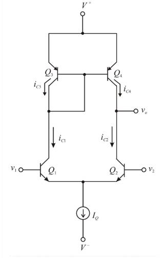
Given bipolar active load diff-amp is,

Given parameters are:
The transistor parameters are:
Calculation:
Let
Since
Now
The collector currents,
Assume that
Assume that
Taking ratio of equations (3), (5) produces,
Taking ratio of equations (4). (6) produces,
From equations (7) and (8)
Substituting equations (1) and (2) in above equation,
Given
Substituting this
(b)
The value of
(b)
Answer to Problem 14.33P
The value of current
Explanation of Solution
Given:
Given bipolar active load diff-amp is,

Given parameters are:
The transistor parameters are:
Calculation:
Let
Since
Now
The collector currents,
Assume that
Assume that
Taking ratio of equations (3), (5) produces,
Taking ratio of equations (4). (6) produces,
From equations (7) and (8)
Substituting equations (1) and (2) in above equation,
Given
Substituting this
(c)
The value of
(c)
Answer to Problem 14.33P
The value of current
Explanation of Solution
Given:
Given bipolar active load diff-amp is,
Given parameters are:
The transistor parameters are:
Calculation:
Let
Since
Now
The collector currents,
Assume that
Assume that
Taking ratio of equations (3), (5) produces,
Taking ratio of equations (4). (6) produces,
From equations (7) and (8)
Substituting equations (1) and (2) in above equation,
Given
Substituting this
Want to see more full solutions like this?
Chapter 14 Solutions
Microelectronics: Circuit Analysis and Design


- A fixed bias n-channel JFET with Vdd= 12V, Rd= 1.2k ohms. Idss=12mA and Vp=-4V. Determine Vs. a.0 V b.None of these c.4.35V d.6.7Varrow_forwardThe Pinch off voltage for N-Channel JFET is -3V, maximum saturated drain current 8mA and the value of VGS is -1.5 V. Calculate drain current, a. 4 mA b. 2.5 mA c. 2 mA d. 18 mAarrow_forwardSolve for the required value of RD, in kOhms to achieve a drain current ID=5.51mA. VDD=15.38V RG=1MOhms VGS(off)=-4.17V IDSS=14.37mA VD=10.22Varrow_forward
- 2.1 A regulator has a no-load output voltage of 12 V and a full-load output of 11.9 V at a load current of 140 mA. Determine the voltage regulation as a percentage change from no-load to full-load and also as a percentage change for each mA change in load current. (6)2.2 What are three types of switching regulators? (3)arrow_forward1) AC power in a load can be controlled by using a. Two SCR's in parallel opposition b. Two SCR's in series c. Three SCR's in series d. Four SCR's in series 2) The advantage of using free - wheeling diode in half controlled bridge converter is that a. There is always a path for the ac current independent of the ac line b. There is always a path for the dc current independent of the ac line c. There is always a path for the dc current dependent of the ac line d. There is always a path for the ac current dependent of the ac line 3) Silicon controlled rectifier can be turned on a. By applying a gate pulse and turned off only when current becomes zero b. And turned off by applying gate pulse c. By applying a gate pulse and turned off by removing the gate pulse d. By making current non zero and turned off by making current zeroarrow_forwardProblem5: For the common base circurt shown in figure find I. and VCB. Assume transistor is Silicon (a-0.98) Ic Rp= 1.5 ko Rc= 1.2 kn VEE = 8 V. Vcc= 18 Varrow_forward
- 3. Write down which transistor structure each curve characteristic belongs to in the figure. Ip -VGS -VGS +VGs (c) VGS (b) (a)arrow_forwardProblem5: For the common base circuit shown in figure find L and Vca. Assume transistor is Silicon.(a=0.98) IE Ic RE= 1.5 kQ Rc= 1.2 k VEE =8 V Vcc= 18 Varrow_forwardIntroduction: For ohmmeter testing purpose, an NPN transistor is similar to two diodes back to back, as shown in figure 12b. there exists two PN junctions, base-emitter and base collector. When each of these junctions is forward biased, the positive lead of the ohmmeter must be connected to P material, and the negative lead to the negative N material (Figure 12c). there should be low resistance reading when these junctions are reverse biased, positive lead to N material and negative lead to P material (figure 12d). The PNP transistor can be tested with a similar method, except that the diodes are face to face as shown in figure 12e. this simple test determines if the transistor is shorted or open on a go (no problems)/no go (it has problems) basis.arrow_forward
- For the circuit given in figure below draw the collector characteristic curves for Ip= 50, 150 and 250 micro amperes on the same graph Re 220 A - Vec 10 V R 10 k Boc= 200 OV-5 Varrow_forwardSolve for Collector Resistance (RC)arrow_forward........ (Figure-1) R. RB= 380kN,Rc= 1kN B = 100, VBB = Vcc=12V RB ww Vec CC ......... I, V CE СЕ V ВЕ BB Q-1-b) Describe briefly the input / output characteristics and application of Common Emitter BJT Configurationarrow_forward
 Introductory Circuit Analysis (13th Edition)Electrical EngineeringISBN:9780133923605Author:Robert L. BoylestadPublisher:PEARSON
 Delmar's Standard Textbook Of ElectricityElectrical EngineeringISBN:9781337900348Author:Stephen L. HermanPublisher:Cengage Learning
 Programmable Logic ControllersElectrical EngineeringISBN:9780073373843Author:Frank D. PetruzellaPublisher:McGraw-Hill Education
 Fundamentals of Electric CircuitsElectrical EngineeringISBN:9780078028229Author:Charles K Alexander, Matthew SadikuPublisher:McGraw-Hill Education
 Electric Circuits. (11th Edition)Electrical EngineeringISBN:9780134746968Author:James W. Nilsson, Susan RiedelPublisher:PEARSON
 Engineering ElectromagneticsElectrical EngineeringISBN:9780078028151Author:Hayt, William H. (william Hart), Jr, BUCK, John A.Publisher:Mcgraw-hill Education,