
Videos
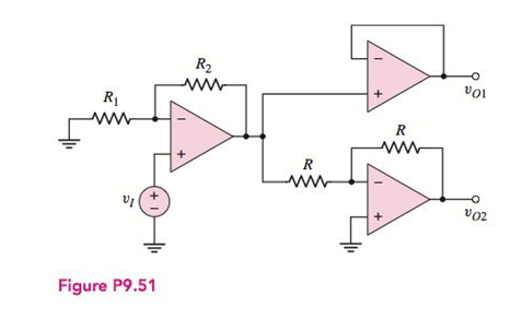
(a) Consider the ideal op-amp circuit shown in Figure P9.51. Determine thevoltage gains
(a)
The expression for the voltage gain
Answer to Problem 9.51P
The relation between the voltage
Explanation of Solution
Calculation:
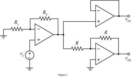
The given diagram is shown in Figure 1
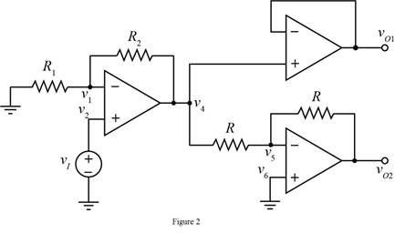
Mark the voltages in the above circuit.
The required diagram is shown in Figure 2
The expression for the value of the voltage gain of first amplifier is given by,
The expression for the value of the voltage gain of second amplifier is given by,
The expression for the value of the voltage
The expression for the value of the voltage
The expression for the voltage
The expression for the voltage
The expression for the voltage
Substitute
The expression for the value of the voltage
Substitute
Apply KCL at node
Substitute
Substitute
Substitute
Apply KVL at node
Substitute
Substitute
Substitute
From above and from equation (1) the relation between the voltage
Conclusion:
Therefore, the relation between the voltage
(b)
The value of the voltage
Answer to Problem 9.51P
The value of the output voltage
Explanation of Solution
Calculation:
The expression for the value of voltage
Substitute
The expression for the value of the voltage
Substitute
Conclusion:
Therefore, the value of the output voltage
(c)
The value of the difference
Answer to Problem 9.51P
The value of the difference of voltage
Explanation of Solution
Calculation:
The expression for the difference
Substitute
Conclusion:
Therefore, the value of the difference of voltage
Want to see more full solutions like this?
Chapter 9 Solutions
MICROELECT. CIRCUIT ANALYSIS&DESIGN (LL)


- Determine the output signal for the op-amp circuit shown in figure below, given Rf1 = 10 km, Rf2 = 5 ΚΩ, R = 1 ΚΩ. . R₁12 R41 #.. www V01 V₁-W V₂ w R Vov 02arrow_forwardI want the answer with details as soon as possible. Please Q-Design an op-amp circuit to amplify the AC voltage of 0.7v to become 3v , And the voltage of VCC is 5v DC.arrow_forward[1] Draw output waveform for the following circuits if sinusoidal signal of 6V peak-to-peak with zero offset is applied at the input. Consider reference voltage VR = +2V D Consider Zener voltage 2.5V v,(1) R VR DY # D₂ R R www. DY VR V₂ (1) vo(1) vo (1) VR = -3Varrow_forward
- Example 07:- For the circuit shown in the figure, calculate the output voltage when 1- R1 = R2 = R3 = R4 = 100 2- R1 = R2 = R3 = 1002 and R4 = 1200 Consider the circuit use an ideal Op-Amp and its resistances do not load the bridge circuit. RA www 12K 10K 10V ww R3 B 122 10K 12Karrow_forwardQ. 79 In the op-amp circuit given in the figure, the load current i, is R₁₂ ww R₁ Vo-W w R₁₂ w R₁ 1°arrow_forwardGraphically show the output voltage (Vo) and load current (IL) by simulating the difference receiving Op-Amp circuit given in the figure.(PSIM using PSpice or)R1 = R2=10kΩRL=1.5 kΩRf=14kΩarrow_forward
- Q1) Using the following input waveform shown in Figure 1, sketch the corresponding output waveform for each op amp circuit shown in Figure 1(a through d). Assume ideal op amp behavior. 30 441 wwwww 25 AG 10 pF 100 k www (6) 1,0 330 www 10 LQ www 51.02 540 M 530 www 10 KO orarrow_forward8) la Ix (Amps) Consider the following circuit and the associated IV curves. Assume that Is = 500fA and VT = .025V. a) Determine when la = 60uA and Vx = 3V. Show your work! b) Determine a when la = 60uA and Vx=3V. Show your work! c) Determine Vbe when la = 60uA and Vx=3V. Show your work! You may use the approximations that were presented in class and additionally you may neglect Va. Ix 8.00E-03 7.00E-03 6.00E-03 5.00E-03 4.00E-03 3.00E-03 2.00E-03 1.00E-03 0.00E+00 0 0.5 Vx 1 1.5 2 2.5 Vx (Volts) 3 3.5 4 4.5 5 ·la = 0 -la = 20uA -la = 40uA la = 60uAarrow_forward3. A generic op-amp circuit is shown in Figure 3. With the given data, answer the following by showing the corresponding circuit and by explaining your answer or presenting the solution. a. If VA-0, VB-1V, RA-RB-10kQ, R1=70kQ, R2=00 and vout-8V, which terminal (A or B) is the noninverting input? b. If VA-10, VB=0V and B is the inverting input, select RA, RB, R1, and R2 and to obtain an output voltage of 20V. c. If VA=VB=1V, R1=0, R2=∞ and Vout=1V, which terminal (A or B) is the inverting input? R2 VA RA OVout RB B VB R1arrow_forward
- 1. For the OPAMP circuit below, assume the OPAMP is ideal. If vi=20sin(10t)-0.2sin(1000t) and v2- v1-20sin(10t) + 0.2sin(1000t). Find the output voltage vo. Find the impedance seen by v1 and the impedance seen by v2 1OR IORarrow_forwardThe DC inputs of the ideal opamp circuit given in the figure are respevtively V1=3V and V2=9V. Calculate output V0 of this circuit.arrow_forwardSolve it op amp...arrow_forward
 Introductory Circuit Analysis (13th Edition)Electrical EngineeringISBN:9780133923605Author:Robert L. BoylestadPublisher:PEARSON
 Delmar's Standard Textbook Of ElectricityElectrical EngineeringISBN:9781337900348Author:Stephen L. HermanPublisher:Cengage Learning
 Programmable Logic ControllersElectrical EngineeringISBN:9780073373843Author:Frank D. PetruzellaPublisher:McGraw-Hill Education
 Fundamentals of Electric CircuitsElectrical EngineeringISBN:9780078028229Author:Charles K Alexander, Matthew SadikuPublisher:McGraw-Hill Education
 Electric Circuits. (11th Edition)Electrical EngineeringISBN:9780134746968Author:James W. Nilsson, Susan RiedelPublisher:PEARSON
 Engineering ElectromagneticsElectrical EngineeringISBN:9780078028151Author:Hayt, William H. (william Hart), Jr, BUCK, John A.Publisher:Mcgraw-hill Education,