
Concept explainers
Videos
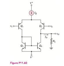
The differential amplifier shown in Figure P 11.60 has a pair of pnp bipolars as input devices and a pair of npn bipolars connected as an active load.
The circuit bias is
Want to see the full answer?
Check out a sample textbook solution
Chapter 11 Solutions
Microelectronics: Circuit Analysis and Design


- 11.13 The i-v characteristic of an n-channel enhancement MOSFET is shown in Figure P11.13(a); a standard amplifier circuit based on the n-channel MOSFET is shown in Figure P11.13(b). Determine the quiescent current ino and drain-to-source voltage vs 2.0 I= 25°C 1.8 1.6 Vas10 V- -9V- 1.4 1.2 8V- 1.0 0.8 7V- 0.6 0.4 5 V= 0.2 3 V- 1.0 2.0 3.0 4.0 5.0 6.0 7.0 8.0 9.0 10 Drain-source voltage vps. V (a) Rp VGD VDD VGS Va Drain current ip, Aarrow_forwardC. Draw a n-p-n transistor connected in circuit common emitter (CE). Draw the input current-voltage characteristic, the output current-voltage characteristics and the graph giving dependence of the output current as function of the input current. Define the amplification gain of this circuit.arrow_forwardPLEASE NEED NOW For the amplifier circuit of the Figure shown below, calculate the voltage gain of each stage, the overall amplifier voltage gain and the output voltage.arrow_forward
- 2. Discuss and compare (by equations) between the relative levels of stability for the following biasing circuits: i. the fixed-bias circuit, ii. the emitter-stabilized bias circuit, iii. the voltage-divider bias circuit, and iv. the voltage-feedback circuit.arrow_forwardFind the following: DC gain, inductor current ripple and output voltage ripple: For DC-DC Buck converter: 1-Draw all circuits in all position 2-Sketch the transistor current waveform 3-Derive analytical expressions for the dc components of the capacitor voltages and inductor currents. 4-Derive analytical expressions for the peak ripple magnitudes of the input filter inductor current and capacitor voltage.arrow_forwardLecturer Karrar Al bayat = Consider the circuit shown in Figure below with transistor parameters ß 120 and VA =00. (a) Determine the small-signal parameters gm, I, and to for both transistors. (b) Plot the dc and ac load lines for both transistors. (c) Determine the overall small-signal voltage gain Av = vo/vs. (d) Determine the input resistance R₁, and the output resistance R.. (e) Determine the maximum Vcc=+12 V undistorted swing in the output voltage. < R₁ = < 67.3 ΚΩ R₂ = Σ 15 ΚΩ Ro R₂ = R₁= 12.7 K 345 ΚΩ Ris Co RC1 = ΤΟ ΚΩ "98 21 REL= <2k2=CE 22 CC3 RE2= RL= 1.6 kΩ < 250 Ω -OUarrow_forward
- Calculate the collector current IC and the emitter collector voltage VCE of the amplifier shown in the figure and determine if it is in active region. shown in the figure and determine if it is in active region. Beta = 150.2. Calculate the input impedance Zi and output impedance Zo if ro = 7.5k.3. Calculate the voltage gain Av of the amplifier.arrow_forward3:A- Explain the AC- analysis of input and output impedance amplifier with negative feedback B:-Voltage gain of common-gate configuration FET amplifier great than (1).arrow_forwardThe DC Current Gain of a Transistor is Select one: a. Ratio of Collector Current to Base Current b. Ratio of Base Current to Collector Current c. Ratio of Emitter Current to Collector Current d. Ratio of Base Current to Emitter Currentarrow_forward
- 9. Design a biased-transistor circuit using VBB = Vcc= 10 V for a Q-point of Ic = 5 mA and VCE 4 V. Assume pc = 100. The design involves finding RB, RC, and the minimum power rating of the transistor. (The actual power rating should be greater.) Sketch the circuit.arrow_forwarda) Calculate the VA voltage value.b) Given the input voltage (Vin) waveformin the above Op-amp circuit, Vtl (low)and Vtu (high) hysteresis crossoverCalculate the voltages. c) At the Vtl and Vtu transitions of the Vo voltageCalculate the position changes.arrow_forwardcircuits by using the small signal models of the transistor. Assume the Early voltage of the transistors are infinitely large. Calculate the small-signal input and output impedances of the following Vcc R1 R1 Rout VB RE Rin R2arrow_forward
 Introductory Circuit Analysis (13th Edition)Electrical EngineeringISBN:9780133923605Author:Robert L. BoylestadPublisher:PEARSON
 Delmar's Standard Textbook Of ElectricityElectrical EngineeringISBN:9781337900348Author:Stephen L. HermanPublisher:Cengage Learning
 Programmable Logic ControllersElectrical EngineeringISBN:9780073373843Author:Frank D. PetruzellaPublisher:McGraw-Hill Education
 Fundamentals of Electric CircuitsElectrical EngineeringISBN:9780078028229Author:Charles K Alexander, Matthew SadikuPublisher:McGraw-Hill Education
 Electric Circuits. (11th Edition)Electrical EngineeringISBN:9780134746968Author:James W. Nilsson, Susan RiedelPublisher:PEARSON
 Engineering ElectromagneticsElectrical EngineeringISBN:9780078028151Author:Hayt, William H. (william Hart), Jr, BUCK, John A.Publisher:Mcgraw-hill Education,