
Videos
For the circuit shown in Figure P5.52, let
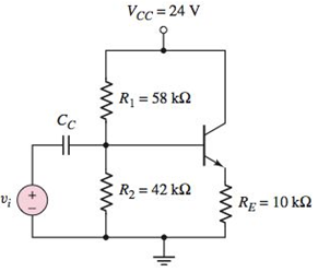
Figure P5.52
a.
The ICQ and VCEQ and then sketching the load line and plotting the Q-point.
Answer to Problem 5.52P
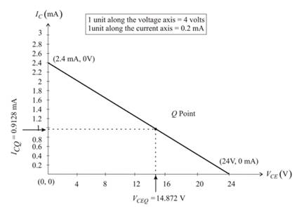
The ICQ and VCEQ :
ICQ =0.9128mA.
VCEQ =14.87V.
Explanation of Solution
Given:
The value of the attenuation factor,
The circuit diagram is shown below:

The Thevenin resistance is evaluated as:
Applying the voltage division rule to evaluate the Thevenin voltage:
Redrawing the given circuit:
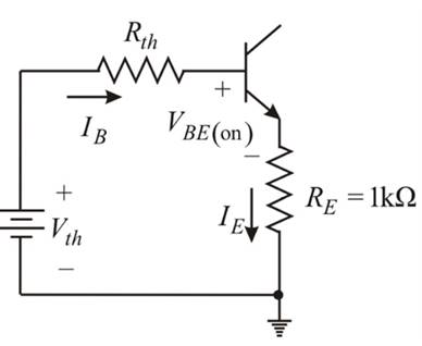
Applying the Kirchhoff’s voltage law in the base-emitter loop:
By the expression of the common emitter current gain:
The quiescent collector emitter voltage is given as:
Hence, the load line equation is given as:
The coordinates of the end points of the load line.
Since, VCE =0-V.
Hence,
Now, substituting IC =0A, then:
Hence, the coordinates of the two extremities of the load line is:
Sketching the load line graph:
b.
The range of the ICQ and VCEQ and plotting the various Q-point on the load line.
Explanation of Solution
Given:
The value of the attenuation factor,
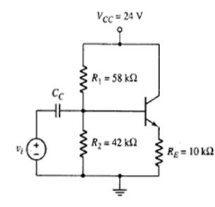
The circuit diagram is shown below:
The resistor R1 and R2 vary by the
Now, evaluating the range of the resistor:
Now, evaluating the range of the R2:
Now taking
as R1 and R2 respectively:
Evaluating the Thevenin resistance using the equation 1:
Applying the voltage division rule to evaluate the Thevenin voltage using the equation 2:
By the use of the equation 3:
Now, from the equation 4:
Now taking
as R1 and R2 respectively:
Evaluating the Thevenin resistance using the equation 1:
Applying the voltage division rule to evaluate the Thevenin voltage using the equation 2:
By the use of the equation 3:
Now, from the equation 4:
Now taking
as R1 and R2 respectively:
Evaluating the Thevenin resistance using the equation 1:
Applying the voltage division rule to evaluate the Thevenin voltage using the equation 2:
By the use of the equation 3:
Now, from the equation 4:
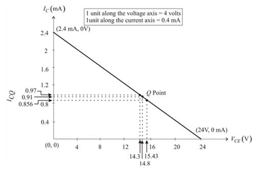
Hence, the plot for the various Q points on the load line is:
Want to see more full solutions like this?
Chapter 5 Solutions
Microelectronics: Circuit Analysis and Design


- IDSS=8mA , VP =-4VTo help plot the DC load line VGS=VG-IDRSa)Attach a Plot of JFET Characteristic Curve as shown in Figureb)What is the approximate VGSQ?c)What is the approximate IDQ in mA?d)Determine source voltage VS.e)Calculate the drain voltage VD.f)Calculate the drain-to-source voltage VDS.arrow_forwardExplain the two types of MOSFETs (draw the physical structure as well). Also explain themajor difference between them regarding mode of operation?arrow_forwardQUESTION 4 In this voltage divider bias circuit, the input is at the base. Output is at the emitter with a high input resistance and low output resistance. The maximum voltage gain is 1 and the coupling capacitors must have a negligible reactance at the frequency of operation. (use to answer a and b) a. Derive the expression for the voltage gain, current gain, and power gain in terms of power delivered to the load, RL. b. Sketch both the DC and AC equivalent circuits. c. Derive the expression for ripple factor of Half Wave Rectification with a capacitor filter.arrow_forward
- Lecture 5 P5.1. For the full-wave rectifier with active load Vrms=120 V, frequency f-60 Hz, load resistor R=5 Ohm. Determine: (1) average load current; (2) average load power; (3) the power factor (PF). (4) maximum voltagearrow_forwardDraw the block diagram of a HVDC converter station and briefly describe the function of each component. Define LCC and VSC and compare their performance.arrow_forwardHow do we know current flows in source terminal? Is this common for n-type mosfet? What is an n-type mosfet?arrow_forward
- For the transistor in Figure P5.38, B = 80. Determine the range in V1 that produces 3 < VCEQ<9V. Vcc = 12 V Rc= 2.2 k2 R = 15 k2 Vow R3 = 100 k2 -12 Varrow_forwarda ): The depletion region is a layer of positive and negative charge in the semiconductormaterial Briefly explain how the depletion region formed in the semiconductormaterial after the PN junction is created.b): An audio signal amplifier is used to reproduce input audio signals at sound-producoutput elements, with desired volume and power levels. What is the function of volumecontrol and power amplifier in an audio signal amplifier ?arrow_forward3. Write down which transistor structure each curve characteristic belongs to in the figure. Ip -VGS -VGS +VGs (c) VGS (b) (a)arrow_forward
- 5.47 The current gain for the transistor in the circuit in Figure P5.47 is B = 60. Determine Rg such that Vo = 8.8 V when V, = 5 V and Ic/Ig = 25. Vec-3v v*-9 V V, ww toro Re= 500 a Van LOV Figure PS.47 Figure PS.48arrow_forwardQUESTION 1 Design a high efficiency 3.3 V, 5A d.c.to d.c. power converter from a 4 to 5.5 Vdc source. The maximum allowable inductor current ripple and output voltage ripple are 0.1A and 20 mV, respectively. Assume a switching frequency of 20 kHz. a) Design a suitable converter power circuit using a MOSFET switch, showing all calculation of inductor and capacitor values and drawing a circuit diagram of the final design including component values. Indicate the peak inverse voltage and forward current rating of any diode required, and the maximum drain- source voltage of the MOSFET. b) On the Schematic diagram, draw the path of the current flow during the ON time and the OFF time. c) Describe the effect of changing the values of the inductor and the capacitor in the circuit. d) What is the effect of switching frequency in the circuit? e) Draw the schematic diagram of a circuit with the output voltage higher than the input voltage.arrow_forward2. We discussed in class how the channel capacitance can be modeled in different region of operations in MOSFETs. For your reference, the slide is shown below. Explain how you think the model would look like if a transistor is in velocity saturation region? Channel Capacitances Channel capacitance is a voltage dependent and non-linear capacitance S C P-sub Bulk Cutoff Region D Operation Region Cutoff Linear Saturation S P-sub Bulk C Linear Region CGBCH CoxWLeff 0 0 1 2 3 S P-sub Bulk Saturation Region CGSCH 0 сат CoxWL eff 1 2 CGDCH 0 CoxWLoft CoxWLoff eff D 0arrow_forward
 Introductory Circuit Analysis (13th Edition)Electrical EngineeringISBN:9780133923605Author:Robert L. BoylestadPublisher:PEARSON
 Delmar's Standard Textbook Of ElectricityElectrical EngineeringISBN:9781337900348Author:Stephen L. HermanPublisher:Cengage Learning
 Programmable Logic ControllersElectrical EngineeringISBN:9780073373843Author:Frank D. PetruzellaPublisher:McGraw-Hill Education
 Fundamentals of Electric CircuitsElectrical EngineeringISBN:9780078028229Author:Charles K Alexander, Matthew SadikuPublisher:McGraw-Hill Education
 Electric Circuits. (11th Edition)Electrical EngineeringISBN:9780134746968Author:James W. Nilsson, Susan RiedelPublisher:PEARSON
 Engineering ElectromagneticsElectrical EngineeringISBN:9780078028151Author:Hayt, William H. (william Hart), Jr, BUCK, John A.Publisher:Mcgraw-hill Education,