
Videos
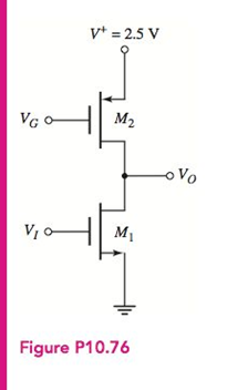
For the circuit shown in Figure P10.76, the transistor parameters are
(a)
The
Answer to Problem 10.76P
Explanation of Solution
Given:
Calculation:
The given circuit is,

The small-signal voltage gain is given, the expression for gain is,
Substituting the given values,
Substitute
Now substitute the given values in above expression,
It is known that,
On putting the given values,
Now substitute the value of
The drain current
Hence
Substitute
Put the value of
Conclusion:
(b)
The voltage
Answer to Problem 10.76P
Explanation of Solution
Given:
Calculation:
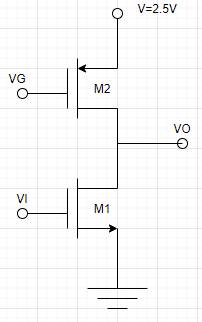
The given circuit is,

The small-signal voltage gain is given, the expression for gain is,
Substituting the given values,
Substitute
Now substitute the given values in above expression,
It is known that,
On putting the given values,
Now substitute the value of
The drain current
Hence
Substitute
Put the value of
Substitute
Conclusion:
(c)
The voltage
Answer to Problem 10.76P
Explanation of Solution
Given:
Calculation:
The given circuit is,
The small-signal voltage gain is given, the expression for gain is,
Substituting the given values,
Substitute
Now substitute the given values in above expression,
It is known that,
On putting the given values,
Now substitute the value of
The drain current
Hence
Substitute
Put the value of
Since
The drain current
On substituting the given values,
Now the gate voltage will be,
Conclusion:
Want to see more full solutions like this?
Chapter 10 Solutions
Microelectronics: Circuit Analysis and Design


- 1. For the circuit in Figure 1: a) Calculate the input and output power if the input signal results in a base current of 5 mA rms. b) Calculate the input power dissipated by the circuit if Rg is changed to 1.5 kN. c) What maximum output power can be delivered by the circuit if RB is changed to 1.5 kN? d) If the circuit is biased at its center voltage and center collector operating point, what is the input power for a maximum output power of 1.5 W? +Vcc (18 V) Rc = 16 2 RB 1.2 k2 V. B - 40 100 µF Figure 1arrow_forwardDraw, Illustrate and label your schematic diagram before solving the problem. 3) Given an Emitter-Stabilize Biased transistor circuit with beta DC is 250,Base resistor is 150 ohms, collector resistor is 1.5k ohms ,emitter resistor is 500 ohms ,emitter voltage supply is -5v and Voltage at common collector is +28V,Voltage at Base-emitter junction is 0.7v,. Determine Base current, Collector current and Voltage at collector-emitter junction.arrow_forwardFind value of RT so that output voltage Vo is (-1.5)(volt).arrow_forward
- circuits by using the small signal models of the transistor. Assume the Early voltage of the transistors are infinitely large. Calculate the small-signal input and output impedances of the following Vcc R1 R1 Rout VB RE Rin R2arrow_forward5, a) Determine Vdsat when ID=.5 mA. b) Determine Kn when ID = 0.5 Amps. (Show your work!) c) Determine VTN. (Show your work!) d) Vgs Consider the circuit and corresponding graph, shown below. ID (mA) 0.60 0.50 0.40 0.30 0.20 0.10 0.00 0 0.5 Vds 1 1.5 2 2.5 Vds 3 3.5 4 4.5 5 -Vgs = 1V - Vgs = 1.1V - Vgs = 1.2V - Vgs = 1.3Varrow_forwardFrom the figure shown, when S1 is at 1 : up position; the following statement is not correct except: (a) Collector-emitter voltage of Q1 is approximately zero (b) the LED will illuminate (c) the base voltage of Q2 is equal to 9 V (d) (b) and (c)arrow_forward
- Using LTSpice, simulate the circuit below, use 2N3904 for the transistor. Part ! DC simulation: Measure VCE and Ic. Use .op for the simulation cmd. Remove all capacitors and input signals first. Part 2 AC simulation: Connect all capacitors now and apply an AC signal at the input with an amplitufe of 1mV and a frequency of 1kHz. Determine the Voltage gain of the circuit by dividing Vo with Vin. Show the output for both the DC and AC analysis. Take a screenshot of the circuit and the output voltages and waveforms. Paste in a word file, write your answers, then save as pdf. 50 kΩ Σ 20 0,5 ΚΩ wwwh 9 Vcc=20 V Ca=1 µF = Cc₂ Cg=50 μF 5.6 kn B=100 Ca IST • 3.3 ΚΩ 5 ΚΩΣ CEarrow_forwardA transistor amplifier circuit is biased so that the quiescent point is to the far left of the load line midpoint. What do you expect to occur when the input voltage begins to vary? O The output voltage will be distorted on the bottom because it will hit the lower limit for VCE before the input voltage arrives at its peak. The output voltage will be distorted on the top because it will hit the upper limit for VCE before the input voltage arrives at its peak. O The output voTransistor's output voltage will look like the input voltage amplified and inverted. The output voltage will be zero (flat).arrow_forwardDetermine V and the made of operation of the PNP transistor showrn in the figure below. Assume l - 10x10 14 A. B- 50, VA -", and R-0.1 KO. Vcc 2V 12V Select one: O a. 0.577 V, Active Mode O b. None of these Oc 2306 V, Saturation Mode O d. 0.23 V, Active Mode O e. 1.153 V. Active Mode < O Oarrow_forward
- 9. Design a biased-transistor circuit using VBB = Vcc= 10 V for a Q-point of Ic = 5 mA and VCE 4 V. Assume pc = 100. The design involves finding RB, RC, and the minimum power rating of the transistor. (The actual power rating should be greater.) Sketch the circuit.arrow_forward% 07 Electronics Pr.. Electronics-Problems Second Sem. 2017-2018 Problem-1 Determine IB, Ic, Ie, VBE, VCE, and VCB in the circuit of Figure below. The transistor has a Bpc = 150. Rc100n Rg Vcc 10 V 10 kn VBB 5 Varrow_forwardA certain npn silicon transistor has vBE=0.7 V for iB=0.1 mA at a temperature of 30°C. Sketch the input characteristic to scale at 30°C. What is the approximate value of vBE for iB = 0.1 mA at 180°C? (Use the rule of thumb that vBE is reduced in magnitude by 2 mV per degree increase in temperature.) Sketch the input characteristic to scale at 180°C.arrow_forward
 Introductory Circuit Analysis (13th Edition)Electrical EngineeringISBN:9780133923605Author:Robert L. BoylestadPublisher:PEARSON
 Delmar's Standard Textbook Of ElectricityElectrical EngineeringISBN:9781337900348Author:Stephen L. HermanPublisher:Cengage Learning
 Programmable Logic ControllersElectrical EngineeringISBN:9780073373843Author:Frank D. PetruzellaPublisher:McGraw-Hill Education
 Fundamentals of Electric CircuitsElectrical EngineeringISBN:9780078028229Author:Charles K Alexander, Matthew SadikuPublisher:McGraw-Hill Education
 Electric Circuits. (11th Edition)Electrical EngineeringISBN:9780134746968Author:James W. Nilsson, Susan RiedelPublisher:PEARSON
 Engineering ElectromagneticsElectrical EngineeringISBN:9780078028151Author:Hayt, William H. (william Hart), Jr, BUCK, John A.Publisher:Mcgraw-hill Education,