EBK ELECTRICAL WIRING RESIDENTIAL
19th Edition
ISBN: 9781337516549
Author: Simmons
Publisher: CENGAGE LEARNING - CONSIGNMENT
expand_more
expand_more
format_list_bulleted
Question
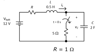
Find iL(0+), vC (0+), diL/dt|t=0+, dvC/dt|t=0+, vC(t). Sketch vC(t) for -0.1 < t < 2 s
A.Draw the equivalent circuit at t = 0- s to find iL(0-) and vC(0-).
B.Draw the equivalent circuit at t = 0+ s with iL(0+) and vC(0+) to find the desired voltages, currents and/or derivatives.
C.Calculate a and w0 and determine type of damping and the form of the solution. If underdamped, calculate wd.
D.Use the initial conditions to determine A1 and A2.
E.Solutions! Sketch vC(t) for -0.1 < t < 2 s.

Transcribed Image Text:Vbatt
12 V
R
L
0.5 H
iL
t=0s
+
502
R = 1 Ω
C
VC
2 F
Expert Solution
This question has been solved!
Explore an expertly crafted, step-by-step solution for a thorough understanding of key concepts.
Step by stepSolved in 2 steps with 1 images

Knowledge Booster
Similar questions
- 5a. What is E2=? 5b. What is E3=? 5c. What is the potential difference of b relative to point a (V_ba)?arrow_forwardFind voltage regulation in typing format please ASAP for the likearrow_forwardPlease try to understand the solution and try to answer in typing format please ASAP for the Plarrow_forward
- An unipolar PWM full bridge circuit has a Vr.rms of 125V at a duty cycle D1 of 0.7. What is Vd? What is Vo.rms?arrow_forwardPeak input voltage =(from graph) ?Peak output voltage = (from graph)?DC voltage across RL = ?ripple factor=?arrow_forwardA voltage commutated chopper operating at 1 kHz is used to control the speed of dc motor as shown in figure. The load current is assumed to be constant at 10 A. 00000 V = 250 V 1₁F XA vous 2mH The minimum time in uses for which the SCR M should be ON isarrow_forward
- how to measure ripple factor and peak input and peak output voltage for this circuits ?arrow_forwardQ1. a) Figure Q1 is a single phase 2-level voltage source converter (VSC) with a total DC voltage V-1000V. A PWM scheme, by comparing a reference value with a 1kHz triangular waveform, is used to control the switches S₁ and S2, and output 340v at Vo. With the aid of graphs explain how pulse signals for the switches are generated, sketch the output voltage Vo, determine the duty cycle and the modulation index. Va + 2 it Va d + TS₁ V {1+5₂ = Figure Q1 A single phase VSCarrow_forward9.38 For a version of the CE amplifier circuit in Fig. P9.11, Ri = 10 k2, R, = 68 kQ, R, = p = k2, and R, = fr= 1 GHz, and C,= 0.8 pF. Neglecting the effect of r, and r, find the midband voltage gain and the upper 3-dB frequency fr 27 k2, R 10 kQ. The collector current is 0.8 mA, ß=200, 2.2 k2, R.= 4.7 %3D sig %3Darrow_forward
- Q1: Draw the d.c load line for the circuit shown in figure. NO SIGNAL VBB Vcc= 12.5 V www Re=2.5 k2arrow_forwardA bridge full - wave rectifier with a capacitor - input filter provides a dc output voltage of 14.5 V to a 330 ohm load. Determine the value of filter capacitor if it connected to input voltage of 12 V rms, 50 Hz. Question 7Answer a. 220 ɲf b. 208 ɲfc. 440 fd. 104 nfarrow_forwardINCLUDE ALL THE DECIMALS.arrow_forward
arrow_back_ios
SEE MORE QUESTIONS
arrow_forward_ios
Recommended textbooks for you
 EBK ELECTRICAL WIRING RESIDENTIALElectrical EngineeringISBN:9781337516549Author:SimmonsPublisher:CENGAGE LEARNING - CONSIGNMENT

EBK ELECTRICAL WIRING RESIDENTIAL
Electrical Engineering
ISBN:9781337516549
Author:Simmons
Publisher:CENGAGE LEARNING - CONSIGNMENT