Introductory Circuit Analysis (13th Edition)
13th Edition
ISBN: 9780133923605
Author: Robert L. Boylestad
Publisher: PEARSON
expand_more
expand_more
format_list_bulleted
Concept explainers
Question
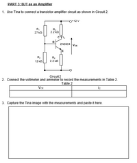
Calculations for Part 3:
- Write down the Input / Biasing Equation:
- Using voltage divider, calculate the voltage, VB.
- Calculate the voltage, VE. Assume VBE = 0.7 V.
- Calculate the current, IC. Assume IC and IE.
- Write down the Output / DC load line Equation:
- Calculate VCE.
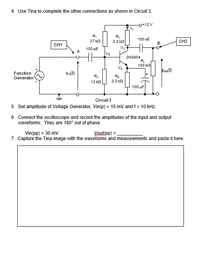
- Calculate the Amplifier Open-circuit Voltage Gain:
AV(OC) = (Vout(OC)(PP) / Vin(PP)) =

Transcribed Image Text:PART 3: BJT as an Amplifier
1. Use Tina to connect a transistor amplifier circuit as shown in Circuit 2.
O+12 V
R,
27 kn
Ro
2.2 ko
cyle
B
2N3904 VcE
E
R2
RE
12 kn
2.2 kn
Circuit 2
2. Connect the voltmeter and ammeter to record the measurements in Table 2.
Table 2
VCE
Ic
3. Capture the Tina image with the measurements and paste it here.

Transcribed Image Text:4. Use Tina to complete the other connections as shown in Circuit 3.
o+12 V
R,
Rc
100 oE
27 kn
2.2 kn
CH2
CH1
B
Ve
100 oE
A
Va
2N3904
R
100 ka
VE
Vadt)
Function
Vin(t)
R2
RE
Generator
12 ka
2.2 kn
100 uF
Circuit 3
5. Set amplitude of Voltage Generator, Vin(p) = 15 mV and f = 10 kHz.
6. Connect the oscilloscope and record the amplitudes of the input and output
waveforms. They are 180° out of phase.
Vin(pp) = 30 mv
7. Capture the Tina image with the waveforms and measurements and paste it here.
Voutipp) =
Expert Solution
This question has been solved!
Explore an expertly crafted, step-by-step solution for a thorough understanding of key concepts.
Step by stepSolved in 4 steps with 4 images

Knowledge Booster
Learn more about
Need a deep-dive on the concept behind this application? Look no further. Learn more about this topic, electrical-engineering and related others by exploring similar questions and additional content below.Similar questions
- Fill in the table VB VC VE Ic LE I8 fre IT gm 5V Consider the circuit given at the right. 600k 1.5k =0.7, Vauo, B=165) 100uF Vo 1k 100uF a) Perform DC analysis and calculate all VB =? VC:? branch currents, node voltages, and small signal parameters 3K VE=? Rout b) Draw a small-signal equivalent model n Vin Rin 400K c) Calculate Ri, Rout, and Ay=Vou/Vin -5Varrow_forward(R₁ = 10k2, Rs = 30kQQ, RG = 100kQ,Vm = 0.8 a) Determine operating point of the circuit. Verify your operation mode assumption. b) Draw small signal equivalent circuit. c) Calculate Rin - d) Calculate Ro. . e) Determine small signal voltage gainarrow_forwardQuestion 4: In the DC/DC Boost Converter shown below, all the components are ideal. Redraw the circuit and show clearly the current path in the loop when: DC Supply Load diode V control RL VOUT VIN FET a) The transistor switch in OFF c) The transistor switch is turned ON after the OFF time of part aarrow_forward
- Q3) The Voltage-divider bias circuit shown below is to be designed to operate efficiently stabilized. Assume Ic(max) = 16mA and VRE= CC: 1) Find the values of R₁, R2, RE, Rc for maximum output voltage swing. 2) Draw the d.c. load line and a.c. load line on same graph indicating the Q point (VCEQ, Ico). 3) Determine the maximum value to which Vcc can be adjusted without exceeding a rating assuming PDmax=400m W Best wishes from me Barwan Ahmed 10 Vino C₁ R₁ www Vcc +20V R2 Rc C3 Si Tr B=100 Vou RL 1karrow_forwardQ2arrow_forwardDiagram show biasing by feedback resistor method.Calculate (i) collector current, and (ii) collector voltage, Given that ß = 100 and transistor is made of sillicon.arrow_forward
- homework multistage Homework: Consider the circuit shown in Figure below with transistor parameters ß 120 and VA =o. (a) Determine the small-signal parameters gm, r, and I, for both transistors. (b) Plot the de and ac load lines for both transistors. (c) Determine the overall small-signal voltage gain Av = vo/vs. (d) Determine the input resistance R and the output resistance Ro. (e) Determine the maximum undistorted swing in the output voltage. Vcc = +12 V RCI = R3= R3 = 15 kQ 10 k2 Ris Ca 67.3 k2 R. Cc3 Deadline: 7-5-2022 SR, = 12.7 k2 REI 45 k2 CE RE2= 3 RL = 1.6 k2 3 250 2 32 k2 ww warrow_forward8.arrow_forwardA. For the configuration shown below in 4(A), find the small signal voltage gain (Voutp-Voutm)/Vin B. For the configuration shown in 4(B), find the following parameters (a) DC value of output voltage, (b) input common mode range and (c) small signal voltage gain when all transistors are in saturation vou/Vin as indicated in the diagram; Assume no body bias on M1 ad M2 For this problem ONLY, assume the following device parameters V7, = \V| = 0.5V;K, = k ,' = 100 µA / V²,a, = a, = 0.01 VDD = 3V (10/1) M, M. (10/1) (10/1) M, |M, (10/1) Voutp 20kΩ м, (200/1) м, м, (10/1) м, Vin (1/1) м, M. (10/1) + Vin DC VAN M, 100HA (1/1) M, M, (10/1) (A) (B) V. =-1Varrow_forward
- answer part b,c, and darrow_forward2) Consider an enhancement MOSFET common source amplifier circuit in Figure 2(a). The output characteristic is showed in Figure 2(b). Assume that the circuit is operating in the saturation region and k = 5 mA/V2. It also given that ra = ro = 00, Cgd = 2 pF, Cgs = 4 pF, Cas = 1 pF, Cwi = 4 pF and Cwo = 3pF. a. Using DC load line, prove that Ino = 22.5 mA and VpsQ = 5.5 V for Vaso = 2.5V. (Please attach the characteristic graph provided in your working solution) b. Draw the AC equivalent circuit at mid frequency. c. Estimate the voltage gain Av = Vo /Vi. d. Determine the dominant high cut – off frequency for the circuit. 10 V Rp 100 2 6 MQ C2 ci Rs RL Vo 1002 R: 5002 Rs Vo 14 MQ Cs 100 2 Vs Figure 2(a) 60- 50 30 20 10 9. 10 Figure 2(b) (yu) 4arrow_forwardFor the p-channel JFET circuit in the Figure, the transistor parameters are: /oss = 2 mA, Vp = |1.75| V. (a) Determine Ipo and Vspo- (b) Give the small signal model (c) Determine the small-signal voltage gains Av = vo/vi QUESTION I: For the p-channel JFET circuit in the Figure, the transistor parameters are: Ioss = 2 mA, Vp = |1.75| V. (a) Determine Ipo and Vspo- (b) Give the small signal model (c) Determine the small-signal voltage gains Av = vo/vi VDD = 10 V Rg = 5 k£2 R1 = 90 kQ %3D Cc2 RL = 10 k2 R2 = 110 k2 wwarrow_forward
arrow_back_ios
SEE MORE QUESTIONS
arrow_forward_ios
Recommended textbooks for you
 Introductory Circuit Analysis (13th Edition)Electrical EngineeringISBN:9780133923605Author:Robert L. BoylestadPublisher:PEARSON
 Delmar's Standard Textbook Of ElectricityElectrical EngineeringISBN:9781337900348Author:Stephen L. HermanPublisher:Cengage Learning
 Programmable Logic ControllersElectrical EngineeringISBN:9780073373843Author:Frank D. PetruzellaPublisher:McGraw-Hill Education
 Fundamentals of Electric CircuitsElectrical EngineeringISBN:9780078028229Author:Charles K Alexander, Matthew SadikuPublisher:McGraw-Hill Education
 Electric Circuits. (11th Edition)Electrical EngineeringISBN:9780134746968Author:James W. Nilsson, Susan RiedelPublisher:PEARSON
 Engineering ElectromagneticsElectrical EngineeringISBN:9780078028151Author:Hayt, William H. (william Hart), Jr, BUCK, John A.Publisher:Mcgraw-hill Education,

Introductory Circuit Analysis (13th Edition)
Electrical Engineering
ISBN:9780133923605
Author:Robert L. Boylestad
Publisher:PEARSON

Delmar's Standard Textbook Of Electricity
Electrical Engineering
ISBN:9781337900348
Author:Stephen L. Herman
Publisher:Cengage Learning

Programmable Logic Controllers
Electrical Engineering
ISBN:9780073373843
Author:Frank D. Petruzella
Publisher:McGraw-Hill Education

Fundamentals of Electric Circuits
Electrical Engineering
ISBN:9780078028229
Author:Charles K Alexander, Matthew Sadiku
Publisher:McGraw-Hill Education

Electric Circuits. (11th Edition)
Electrical Engineering
ISBN:9780134746968
Author:James W. Nilsson, Susan Riedel
Publisher:PEARSON

Engineering Electromagnetics
Electrical Engineering
ISBN:9780078028151
Author:Hayt, William H. (william Hart), Jr, BUCK, John A.
Publisher:Mcgraw-hill Education,