+VDD Rp Rp Upi "p2 + vOD M1 M2 +. U2 Iss --Vss (b)
Q: a) AK type thermocouple is utilized in the figure given below. The reference temperature (cokd…
A:
Q: For a certain 4-bit successive-approximation ADC, show the step-by-step conversion of a constant…
A: 4-bit successive-approximation ADC: The block diagram of a 4-bit successive-approximation ADC is…
Q: Our calculation of the input resistance of the common-gate and common-base amplifiers neglected ro…
A:
Q: Consider the differential amplifier shown in Figure P11.3 with transistor parameters B = 150,…
A: Given data:
Q: Design a 4-bit DAC assuming high voltage of 3.5 V and a Vcc of 12 V? determine the output voltage…
A:
Q: A power switching device of current gain = 100, load resistance = 0.5 KM, consider the maximum load…
A: Given, Current gain (β)=100 , Load Resistance RL=ROUT=0.5KΩ=500Ω Supply Voltage V=5V, Solenoid…
Q: For the Differential amplifier shown:, calculate the following: 1. The differential mode gain 2.…
A: Here, we have given a differential amplifier. The values of electric current density are defined in…
Q: Consider a 6 bit DIA converter with a resistance of 320 kΩ in LSB position. The converter is…
A: Digital to Analog converter- A “D to A Converter” or DAC translates a digital code into the…
Q: (a)Find the Q-points of the transistors in the CMOS op amp shown if VDD = VSS = 5 V, IREF = 250 μA,…
A: From the given circuit.
Q: Q4) For the circuit shown below, the output voltage (10.01005 volt). If the differential gain (Ad)…
A: Given that
Q: Draw the DC equivalent circuit, then determine Ic and VCE.
A:
Q: Q.1 State a reason why we need to use more emitter-follower and a voltage divider instead of one…
A:
Q: Q3: Using 4-bits successive approximation A/D converter, explain with sketching the required figures…
A: A combinational circuit is one in which the various gates in the circuit, such as the encoder,…
Q: Draw small signal equivalent circuit and derive expression of voltage gain RD R Vo Cc R2 Rs -5 V ww…
A: MOSFET(Metal Oxide Semiconductor field effect Transistor) is three terminal electronic device.…
Q: Can a 74AS138 output drive a 74AC08 input when both are supplied with Vcc = 4.5V? Why or why not? Be…
A: the correct answer is yes.lets see how
Q: What is the output current of the VBEbased reference in the given figure if R1 = 20 kN, R2 = 20 kN,…
A:
Q: A differential amplifier has a common-mode gain (Ac) of 0.2 and a common-mode rejection ratio…
A:
Q: 5. Calculate the overall gain and noise figure for the system shown in figure below. Р, - зав G,-…
A: Given: Overall gain G=G1+G2=20+20=40 dB
Q: Draw the internal circuit diagram of uA741 Op-Amps.
A: Explanation: The internal circuit of IC UA741 is So we can see there is only one Op-Amp in the…
Q: write about Binary weighted resistor DAC (diagram, construction, operation applications )
A: “Since you have posted a question with multiple sub-parts, we will solve the first three sub-parts…
Q: The CMOS op-amp is fabricated with the process such that = 24V/um. If the length of the transistors…
A: In the question given the values of using parameters for the fabrication of the CMOS op-amp and…
Q: What are the output current and output resistance of the current source as shown if VDD = 4 V, R4 =…
A: Given VDD=4 VR4=200 kΩR3=100 kΩRs=16 kΩ The expression for equivalent voltage is given by…
Q: For an active-loaded MOS differential amplifier shown in Figure 2, assume that for all transistors,…
A:
Q: Estimate the differential-mode gain, common-mode gain, and CMRR for a differential amplifier with…
A: Given VCC=15 V Add=-20VCC The overall differential mode gain equals to Add, in differential output.…
Q: Consider the amplifier shown in FigureP13.61 . With zero dc input voltage from the signal source, it…
A: (a) The below figure shows the zero dc input voltage from the signal source with including the…
Q: Q4 (a) A class B push-pull amplifier having a Vcc = 20 V and R1 = 10 N. (i) Derive the equation for…
A: A class B push-pull amplifier has Vcc=20 V and RL=10 Ω. i) We need to derive the equation for the…
Q: 1. A five-bit D/A converter produces VOUT = 0.2 V for a digital input of 00001 a)Sketch a potential…
A: According to the question, for the five-bit DAC, we need to find (a) Resolution, when Vout=0.2 V for…
Q: a) For the differential amplifier circuit of Fig. Q4a, le 47 kn Rc Ro 47 kr Ver Ve Q, B= 75 Van 2 mv…
A: Bartleby has policy to solve only first 3 subparts of a question. Please reupload the question.
Q: A. Consider the Common-Source (CS) amplifier shown below. Vo He Cc Rsig CG RL Cs Sketch/draw and…
A:
Q: For the NMOS circuit below, VDD = 9V, Vt = 1V, kn = kn’(W/L) = 2mA/V2 . Neglect channel length…
A:
Q: For an eight-bit D/A converter having a range of 5 V, convert 10110110 into an analog sample value…
A:
Q: The JFET amplifier shown must develop a 10-V peak-to-peak sinusoidal signal across the 18-kΩ load…
A: According to question: ∵id=VDSRD+gmVGSAt…
Q: Use SPICE to simulate the amplifier shown and compare the results to hand calculations. Use…
A: The given circuit is,
Q: - A 5-bit DAC has a current output. For a digital input of 101000, an output current of 10mA is…
A:
Q: Q2// Amplifier cct. Shown below is designed to give maximum symmetrical swing if current gain ß that…
A: a Apply voltage division rule,⇒VB=VBB=15×RBRB+Ri⇒VBB=15×1010+1=13.63 VFrom base…
Q: (a) Determine IC1, VCE1, and hiej of QI. (b) Determine Ic2, VCE2, and, hie2 of Q2. (c) Determine Zin…
A: "According to the Comapny's policy we will solve the first three parts of the question". Given the…
Q: 1. Enhancement Type MOSFET 2. Depletion Type MOSFET Construction Systematic Diagrams Working…
A: MOSFET stands for Metal oxide silicon field effect transistor, It is used in switching and…
Q: Q.1 a. State a reason why we need to use more emitter-follower and a voltage divider instead of one…
A:
Q: Given: Cascode Amplifier ... VDD R1 = 7.5 kQ R2 = 6.8 kQ R3 = 4.7 ka Rc = 2.2 kQ RE = 1.2 kQ Vcc =…
A:
Q: 13.The maximum deviation between actual and ideal converter output after the removal of error is a)…
A: DAC is used to convert digital signal to analog signal ADC is used to convert analog signal to…
Q: 3. Given a 4-bit DAC with the input/output table below, with a 10V Vref. (a) What is the offset…
A: 3. Given a 4-bit DAC with the input/output table below, with a 10V Vref. (a) What is the offset…
Q: The CMOS op-amp is fabricated with the process such that V = 24V/µm. If the length of the…
A: Given data Length of the transistor is L = 0.5 μm DC open loop gain is 4600 V/V Voltage is VA' = 24…
Q: The two-stage CMOS op-amp shown in the figure below has: • Reference current I- 191 µA, (W/L)1 =…
A: Given: I=191 μA , Early voltage |VA|=102 V for all transistors. μnCox=53 μA/V2and μpCox=21 μA/V2.…
Q: V* = 10 V Rp Ip M. M V=-10 V
A:
Q: 4. a) Why do we need Q1 and Q2; b) List all current mirrors Figure 4 shows two-stage CMOS op-amp.…
A: Current mirror: The current mirror is used to design the constant current source and this is very…
Q: For the Differential amplifier shown:, calculate the following: 1. The differential mode gain 2.…
A: The answer as given below:
Q: Solve
A: Redrawing the given circuit by marking the inverting and non inverting voltage:
Q: A 741 op amp is manufactured in an 8-pin dual-in-line package. What are the terminal num- bers for…
A: to find the terminal numbers
Q: Q4: Consider the uA741C-based op-amp amplifier circuit shown below; The input voltage, Vi, is 2.5…
A: Given data R1=1000 R2=5000 Vi=2.5
Q: IB, Ic. le, Vceq, Ve find the values. By plotting the load curve of the circuit Specify the…
A: We will do dc and analysis to calculate unknown parameters .
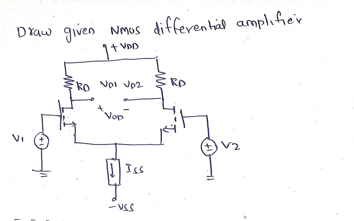
Draw a PMOS version of the NMOS differential amplifier as shown.
Step by step
Solved in 2 steps with 2 images
- Reconsider Problem 3.29. If Va,VbandVc are a negative-sequence set, how would the voltage and current relationships change? (a) If C1 is the complex positive-sequence voltage gain in Problem 3.29 and (b) if C2 is the negative sequence complex voltage gain, express the relationship between C1andC2I want Introducrion for ( MEASUREMENT USING DC BRIDGES ) by using Resistance Measurement using DC Bridges , Resistance Measurement using the Wheatstone Bridges and Resistance Measurement using the Kelvin Doubles Bridges ) please write the introduction in print font to copy it ?What is Ohms law? Explain with examples
- 2:34 ull 4G I moodle1.du.edu.om An RTD forms one arm of a Wheatstone bridge as shown in the figure. The RTD is used to measure a temperature with the bridge is operated in a balanced mode. The RTD has a resistance of 252 at a temperature of 0°C and a thermal coefficient of resistance a=0.003925C-1. The value of the variable resistance R, must be set to 41.485 Q to balance the bridge circuit. Determine the temperature measured by the RTD where R2=R3=1002 R2 R3 RTD RRTD E, Select one: O a. 4200Rectifier Circuit. 1. What is V1 reading? a. 110V b. 220V c. 0V d. 146.67V 2. What is V2 reading? 146.67V 207.42V 0V 103.7V 3. What is V3 reading? 132V 104V 207.42V 147V Thank u.Known Vsat for LM741 ± 14V for source voltage Vs ± 15V. If Vi1 = 3 V and Vi2 = 4 V, Ri1 = Ri2 = Ro2 = 1 K Ohms. Define what is the value of Vo? how much
- Q2. Perform the following subtraction using l's and 2's complement method (Show step by step process) (i) (11010)2 – (10100)2 (ii) (1000101)2 – (1010100)2what is ripple ? how to minimize the rippl , draw the circuit and show ??93 Two conductances G₁ and. G₂ having values of 600 and. Yoo S respectively. are connected in paralled.. The combination is then corrected in parallel with 800 resistor. Calculate thes a) Equivalent resistance of the parallel circuit. [Ans: 363-63-53 b) Current in each branch if Gy_Carries 2mA. [Ans: 3m 4:16m) c) power dissipated in each branch-[Ans: 6.6mw, lamws13-8mm- d) Voltage across each somponent- [Anse 3-33-v]. e) Total power dissipated: (Ans: 30-5. mwt
- Q1. a) An SCR based AC power controller circuit is given in Figure 1. The circuit connects a 240V 50Hz AC source vi to a resistive load with resistance of 100. If the delay angle is a-15°, draw the waveforms of the load voltage Vo, and the voltage across SCR2. Calculate the power supplied to the load. + Vi Va + 2 SCR2 H₁₁ SCR₁ Figure 1 SCR based AC power control circuit Va + 2 io b) Figure 2 is a single phase 2-level voltage source converter (VSC) with a DC voltage Vd-200V. A PWM scheme, by comparing a reference value with a 10kHz triangle waveform, is used to control the switches S₁ and S2. The modulation index of the PWM is m=0.8. With the aid of graphs explain how pulse signals for the switches are generated, sketch the output voltage Vo, determine the duty cycle, and calculate the average output voltage. + Vo + Vo √ ₂ == Figure 2 A single phase VSCb) Use the ALU 74181 in the figure below and the tables (one is enough; second maybe, need to check the new kit) to implement : A + B, A – B, A. B. (MSB) (LSB) 10 (MSB) F3 F2 F1 FO S3 Cn+4 16 s2 20 U14 15 S1 14 so A3 A2 A1 AO B3 B2 B1 B0 M Cn 24 23 22 21 28 27 T26 25 (LSB) (MSB) (LSB)(MSB) (LSB) And given that under M = 1 the circuit performs the following arithmetic and logic functions according to Table 11.1. Input selection S3 Output M-H S2 SI Cn=L. F3 F2 F1 FO A 1 -A В -B A&B AxB 1 A'B 1 Ax(-B) (-A)xB (-A)x(-B) 1 1 ACTIVE HIGH DATA M-L: ARITHMETIC OPERATIONS SELECTION M-H LOGIC s3 s2 s1 so Ino carry) (with carry) F-A PLUS 1 F- LA + B) PLUS 1 F- (A + BI PLUS 1 FUNCTIONS L L F-A F-A+B F-AB F-A H FA+B F-A+T F- MINUS 1 12s COMPL) F-A PLUS AB F- IA + BI PLUS AB L L L L F-0 F-ZERO F- AB F-A PLUS AB PLUS 1 F- (A + BI PLUS AB PLUS 1 L L L H L F-AOB F- AB L L F-A MINUS B MINUS 1 F-A MINUS B F- AB MINUS 1 F- A F-A PLUS AB PLUS1 F-A PLUS B PLUS 1 F- IA + B PLUS AB PLUS 1 L H L F-A PLUS AB…For an RTD the relationship between resistance and temperature is a. proportional b. no relation c. equal d. inversely proportional