Electric Motor Control
10th Edition
ISBN: 9781133702818
Author: Herman
Publisher: CENGAGE L
expand_more
expand_more
format_list_bulleted
Question

Transcribed Image Text:UIComplement binary number P by
35, i.e. F = P x 35. Using only adders and shifters, show how t
8 UTM
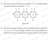
(c) Figure Q.3.2 shows a 3-bit ripple-carry-adder for S= A + B. Modify the adder
8 UTM O
to perform the subtraction operation F = A – B.
& UTM
TM & UTM
A2
B2
A1 B1
3 UTM
Ao
Bo
TM &UTM 3 UTM
Cout
FA
8 UTM & UT
FA
Co
FA
TM & UTM & UTM
S2
&UTM & UT"
8 UTM
So
Figure Q.3.2
UTM &UTM
Assume that you need to multiply an 8-bit
UTM
Td)s UTM UTM
UTM & UT
35, i.e. F = P x 35. Using only adders and shifters, show how the operation can
UTM 5 UTM
2's Complement binary number P by
, UT
- UTM 5 UTM
& UTM &U
- UTM 5 UTM
& UTM &UT
UTM 5 UTM
UT"
Expert Solution
This question has been solved!
Explore an expertly crafted, step-by-step solution for a thorough understanding of key concepts.
Step by stepSolved in 4 steps with 2 images

Knowledge Booster
Learn more about
Need a deep-dive on the concept behind this application? Look no further. Learn more about this topic, electrical-engineering and related others by exploring similar questions and additional content below.Similar questions
- Nonearrow_forwardBelow is an example of an NMOS logic circuit. For all of the MOSFETs in the circuit below, assume V = 1 V and k = 50 mA/V². th W R₂ = 5600 PEETHIPPIN R₁ - 4700 M3 M₁ M. 0 a. Indicate and verify the state of each MOSFET and V for the following input combinations. Fill-out the table below for each assumed state of the MOSFET for every input combination. Use R approximation for linear operation and three significant ds(on) figures for the voltages. 오 Ao SV whyarrow_forwardI need solution details in 30 minutesarrow_forward
- What will be the boolean function (y) for the given CMOS logic circuit as shown in the figure? AMP, MP₂-B MP3 A—IL MN, BCMN₂ D- V₂ HCMN₂ DD MP -D MP-E y MN3C GND MNEarrow_forwardThe principle of carry look ahead is used to speed up a ripple adder. a. b reduce the number of inputs of binary adders. simplify the design process of binary adders. d. validate the outputs of a ripple adder. none of the others. e.arrow_forwardQ1: Write a Verilog code for the 16 bit ripple carry adder. The hierarchy of 16-bit ripple carry adder is sbown in figure below. The ripple cary adder is made up of four 4-bit full adder, each 4-bit full adder is made up of four full adders which in turn made up of two half adders and OR gate. Fimally each half adder is made of xor, nand and not gate. Add ma 16 Add ns_4 Add pe_4 Add rca_4 Ad a4 MI Add ful Add ful Add_full Adil f Ad Aul Ad hal sandarrow_forward
- In a simple, three-phase voltage-source inverter of the form shown in Fig. 8.18, the direct voltage va in the link is 550 V. The frequency of the inverter output is 200 Hz. Determine: (a) the rms value of the fundamental component of the output voltage, line to line and line to neutral, and (b) the rms value of the actual output voltage line to line and line to neutral.arrow_forwardneed help with digital logicarrow_forwardDigital logic design Solve it with drawing and simulation lab I need them both to have the full solution. And thanks Design counter that counts from 00 to 59, using the IC 74LS90 ripple counter and use two 7 segment display to display the result count. You can also use 7447 binary to 7-segment Display Decoder.arrow_forward
- Introduction to Logic design EENG115. Please solve it by introduction to Logic design onley and make your Line clear and step by step pleasearrow_forwardPlease do part b using the Assumptionarrow_forwardA 12-bit D/A converter has a full scale voltage of 10.00 V. What is the voltage corresponding to the LSB? To the MSB? What is the output voltage if the binary input code is equal to (100100100101)?arrow_forward
arrow_back_ios
SEE MORE QUESTIONS
arrow_forward_ios
Recommended textbooks for you
