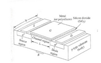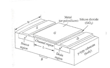
Refer to the generic FET figure for this problem. And choose the correct answer inside the parenthesis
(a) If the substrate doping is NA = 5 x 1016 cm-3, the basic
structure is (CMOS, PMOS, NMOS, JFET, MESFET) and the inverted
channel charge carriers are (HOLES, ELECTRONS, BOTH HOLES
AND ELECTRONS, NEUTRONS, PHOTONS).
(b) If the substrate doping is changed to be ND = 5 x 1016 cm-
3, the basic structure is (CMOS, PMOS, NMOS, JFET, MESFET) and
the inverted channel charge carriers are (HOLES, ELECTRONS, BOTH
HOLES AND ELECTRONS, NEUTRONS, PHOTONS)
(c) Assume L = 50 nm, W = 500 nm, tox = 200 Å. Units are important!!!!!!
Compute Cox and Compute CTotal

Given the internal structure of FET:

a) If the substrate doping is NA = 5 x 1016 cm-3, then we need to find what is the basic structure out of the options( (CMOS, PMOS, NMOS, JFET, MESFET) and also we need to find the inverted channel charge carrier out of the options(HOLES, ELECTRONS, BOTH HOLES AND ELECTRONS, NEUTRONS, PHOTONS).
b) If the substrate doping is changed to be ND = 5 x 1016 cm-3, then we need to find what is the basic structure out of the options( (CMOS, PMOS, NMOS, JFET, MESFET) and also we need to find the inverted channel charge carrier out of the options(HOLES, ELECTRONS, BOTH HOLES AND ELECTRONS, NEUTRONS, PHOTONS).
c) Assuming L = 50 nm, W = 500 nm, tox = 200 Å. We need to compute Cox and CTotal.
Step by stepSolved in 4 steps with 2 images

- 6. For a particular dual-slope ADC: Vref = +5.0V and the charge time is 6ms. %3D a) " Draw a time-domain plot for the dual-slope ADC. b) When Vin = -2.5V, what is the total conversion time? c) When Vin increases by 1.0V, what is the total conversion time?arrow_forwardA silicon diode made, half-wave rectifier produces a maximum value of load current as 20 mA through a resistance of 1 KQ. What is the PIV of the diode?arrow_forwardA 0.4 W zener diode is rated to have VzT = 5.1 V at a test current of IZT 6 mA. Its incremental resistance rz 13 Ohms. = = (a) What voltage will result when conducting a reverse current of Iz (b) What is the maximum safe current, assuming the test zener voltage is constant? = 19 mA? (c) What is the maximum safe current, using the linearized model and including the effect of r₂?arrow_forward
 Introductory Circuit Analysis (13th Edition)Electrical EngineeringISBN:9780133923605Author:Robert L. BoylestadPublisher:PEARSON
 Delmar's Standard Textbook Of ElectricityElectrical EngineeringISBN:9781337900348Author:Stephen L. HermanPublisher:Cengage Learning
 Programmable Logic ControllersElectrical EngineeringISBN:9780073373843Author:Frank D. PetruzellaPublisher:McGraw-Hill Education
 Fundamentals of Electric CircuitsElectrical EngineeringISBN:9780078028229Author:Charles K Alexander, Matthew SadikuPublisher:McGraw-Hill Education
 Electric Circuits. (11th Edition)Electrical EngineeringISBN:9780134746968Author:James W. Nilsson, Susan RiedelPublisher:PEARSON
 Engineering ElectromagneticsElectrical EngineeringISBN:9780078028151Author:Hayt, William H. (william Hart), Jr, BUCK, John A.Publisher:Mcgraw-hill Education,


