Rc RC Ссвы 2 k2 2 k2 Ccsi Ces2 Сси Сскеа VREF I1.7 k2 42 k2 42 k2 -VFE = -5.2 V
Q: Show your solutions clearly and systematically. The D latch of Figure 1 is constructed with four…
A: D Latch: Latch is an electrical device that can store a single piece of data. The D latch is used to…
Q: Simplify the given Boolean function and design its logic gates(NAND and NOR) with the help of…
A: Simplify the given Boolean function and design its logic gates(NAND and NOR) with the help of…
Q: For a two-input gate, the standard SOP expression is Y = A'B + AB' +AB O a. NAND O b. EX NOR O c.…
A: The SOP expression is the sum of product expression. The OR function of a variable and it's…
Q: if332to base10=x to base8 then find the value of X.(c)1001011.0112 to equivalent decimal
A:
Q: Draw breadboard for 4-bit Piso connection regis ter using D flip-Flop IC with its along pin…
A: To give the breadboard connection
Q: 4. A 4-input MUX is shown on the left below. The logic gate diagram is shown below it, FYI. For the…
A: For the given multiplexer circuit we have to complete the timing diagram
Q: 2- Given a BCD decade counter, show the decoding logic required to decode each of the following…
A: (a) For getting HIGH output when the counter counts 0110, the decoding logic needed for decoding the…
Q: Determine the output Q in each of the following logic diagram 7. A=1, B=0 then Q=? 8. A=1, B=1, then…
A:
Q: Simplify the Boolean function and design its logic gates(NAND and NOR). F1(x,y,z) = xy’z+xyz+y’z’
A: Simplifying the given boolean function.…
Q: Determine the output Q in each of the following logic diagram 1. A=1, B=1, C=1, D=0, then Q=? 2.…
A:
Q: (Short-answer Question) Given a BCD decade counter with only the Q outputs available, show what…
A: (a) For getting HIGH output when the counter counts 0110, the decoding logic needed for decoding the…
Q: The IC number of the logic gate which is the complement of X-NOR gate is 7432 O 7404 O 7486 O 7400
A: Complement of XNOR gate is XOR gate. First we will consider each of the IC number separatly to…
Q: The D latch of Figure 1 is constructed with four NAND gates and an inverter. Consider the following…
A: Solution- = DC'.C'= DC+C'=D+C' C+C'= D+C'
Q: The IC number of logic gate which is complement of X-NOR gate is O a. 7404 O b. 7400 O c. 7432 O d.…
A: Complement of Xnor gate is Xor gate .
Q: What is the output of an N input XOR gate if the number of input with logic l' is even? a. unknown…
A: For XOR gate, 1 is the output of an N input XOR gate if the number of input with logic 'I' is even…
Q: Determine the output Q in each of the following logic diagram 5. A=1, B=0 then Q=? 6. A=1, B=1, then…
A:
Q: For the basic TTL gate shown in figure (5), if logic (1), BR = 0.02 and Br = 100, then find the v…
A:
Q: (b) Compute the logic effort and parasitic delay of the following gates (assume Hn= 2µp): |(i) 3…
A: Note: We are authorized to answer one question at a time since you have not mentioned which question…
Q: Q17. i) For the Figure Q17, find the logic function Z lo 4 TO 1 1 to 4 X, DEMUX X2 1- MUX I2 So C.…
A: In this question , we will find output and truth table...
Q: 1. Use two NOR gates to construct basic SR latch circuit shown in Figure 1. Connect R and S inputs…
A: Since the SR latch is built using Nor gates it is active high SR latch. Considering the initial…
Q: Create the logic fora cnebit addition circuit. Inputs are X, Y,Co Xand Yare the bits being added.…
A: Draw the truth table for the above addition variables. Inputs Outputs X Y Cin Sum…
Q: The IC number of logic gate which is complement of X-NOR gate is O a. 7404 O b. 7432 O c. 7486 O d.…
A: Compliment if XNOR gate is XOR Gate. XOR gate has IC number 7486.
Q: A dairy factory uses an 8255 PPI card at base address 5000 H. a) Explain how port address is changed…
A: Given that: Port A=Output Port B=Input Port C lower=output Port C Upper=Input By default Mode 0 is…
Q: Scale the transistor sizes to decrease the gate power by a factor of 8. (b) Scale thetransistor…
A: Concept: A capacity to do work is called energy and it may exist in potential, kinetic, thermal,…
Q: The following circuit is to be used to implement the function f(X,Y,Z) = XZ. Determine which of the…
A: The following circuit is to be used to implement the function f(X,Y,Z) = XZ. Determine which of…
Q: The IC number of logic gate which is complement of X-NOR gate is a. 7432 O b. 7486 7404 O d. 7400
A: IC 7432 -OR gate
Q: Consider 4-bit input Decoder, (i) The output pins are equal to .. (ii) how many logic gates in the…
A: 4 bit input decoder Decoder have output pine = 2n n no of bit. The output pine? Logic gate…
Q: 1 Use feed - forward structure, and check the correctness of weight coefficient for the logic gate…
A:
Q: Using only the 2-input NAND gates, what is the minimum number of gates that is needed to implement…
A: Given Boolean function, F=x+y'+x
Q: The IC number of logic gate which is complement of X-NOR gate is O a. 7400 O b. 7404 O c. 7486 O d.…
A: The IC number for the X-OR gate is 7486. In this IC there are 4 gates on this package, each with 2…
Q: Draw the full logic diagram of an octal-to-binary priority A (LSB) 1+3+5 +7 1.2 .+3..+ B -…
A: Let D0 to D7 be the inputs of the priority encoder. Write the truth table for the above encoder.…
Q: Identify each of these logic gates by name, and complete their respective truth tables: :D Ostput…
A:
Q: +12V 15K 2.2k D1 oVo A 15k D2 100k -12V ver the following questions for the given circuit: Prove…
A:
Q: Short-answer Question) Given a BCD decade counter with only the Q outputs available, show what…
A: for the given BCD decade counter with only the Q outputs, given that, (a) 0001 (b) 0011 (c) 0101…
Q: Fill in the blanks in the truth table of the given digital circuit. Use for NOT gate egX. Use…
A: Here 7 gates were used Gate 1 AND gate Inputs X, Y, Z output = XYZ
Q: Which of the following logic gates have only one I/P and one O/P? O a. AND GATE Ob. NOT GATE Oc.…
A: The Answer is NOT gate and is explained below in detail.
Q: 5) Realize the following functions using decoder and logic gates. a. Implement f(w1,w2,w3) = m…
A: If we take OR of the outputs of the active high decoder, it gives the SOP form of the function, F.…
Q: ERIMENT MANAL 6. How many basic logic gates are required to construct a XOR gate? 1.4 2.5 3.6 17.…
A: The solution can be achieved as follows.
Q: AB EXPERIMENT JAL 6. How many basic logic gates are required to construct a XOR gate? 1.4 2.5 3.6
A:
Q: Design and draw out a decoder at the gate level that enables the 4 logic blocks shown below. The…
A: A decoder has few inputs and many outputs. If its inputs are 'n' and its output will be 2n. Only one…
Q: SW1 SW2 L1 L2 A B 1 2 4 5 1 1 2 3₂. 6 9 10 3 8 What logic function is being performed? وان C L3
A: Today, logic gates are found in the majority of the electrical equipment people use. For instance,…
Q: A 3-to-8 decoder can be built using two 2-to-4 decoders plus some basic logic gates as shown in the…
A:
Q: Demonstrate perceptron learning of the binary logic function OR, where the threshold e=0.2, learning…
A: A neuron is a mathematical function that is based on the way biological neurons work. In an…
Q: on BE RA= 0.7V, V, (sat) 0.8V, Vcz (sat = 0.15V,V SED on) =0.3V, 0 = 0.85, B = 0.25 BC BE Q4. Open…
A: open collector logic gate is shown above and which logic function is performed here
Q: INPUT OUTPUT A AND NAND OR NOR XOR XNOR 1 1.
A: Logic gates are used for logical calculation or logical expressions when we are provide binary…
Q: What is the simplified algebraic expression for the logic gate sho Doz X C Y OX+Y OX.Y OX.Y ΟΧΘΥ…
A:
Q: Imagine the output of IC 7404 can feed a maximum of five LED's, then which of the following…
A:
Q: Consider the full adder implementation shown below, and the corresponding delays of the gates.…
A: Propagation delay. It is the maximum time taken by the gate from the input signal given to the come…
Q: How many number of binary input combinations are possible for a 3-input gate ? 8 16 2 4
A: No.of possible combinations for n input gate is 2n
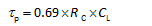
What are the delay and power-delay product for the ECL gate as shown if IEE is changed to 0.5 mA, but the logic swing is maintained the same?
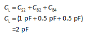
Determining delay of the ECL gate is
Determining effective load capacitance for collector mode
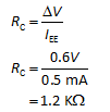
Determining load resistance
Step by step
Solved in 2 steps with 6 images
- b) Use the ALU 74181 in the figure below and the tables (one is enough; second maybe, need to check the new kit) to implement : A + B, A – B, A. B. (MSB) (LSB) 10 (MSB) F3 F2 F1 FO S3 Cn+4 16 s2 20 U14 15 S1 14 so A3 A2 A1 AO B3 B2 B1 B0 M Cn 24 23 22 21 28 27 T26 25 (LSB) (MSB) (LSB)(MSB) (LSB) And given that under M = 1 the circuit performs the following arithmetic and logic functions according to Table 11.1. Input selection S3 Output M-H S2 SI Cn=L. F3 F2 F1 FO A 1 -A В -B A&B AxB 1 A'B 1 Ax(-B) (-A)xB (-A)x(-B) 1 1 ACTIVE HIGH DATA M-L: ARITHMETIC OPERATIONS SELECTION M-H LOGIC s3 s2 s1 so Ino carry) (with carry) F-A PLUS 1 F- LA + B) PLUS 1 F- (A + BI PLUS 1 FUNCTIONS L L F-A F-A+B F-AB F-A H FA+B F-A+T F- MINUS 1 12s COMPL) F-A PLUS AB F- IA + BI PLUS AB L L L L F-0 F-ZERO F- AB F-A PLUS AB PLUS 1 F- (A + BI PLUS AB PLUS 1 L L L H L F-AOB F- AB L L F-A MINUS B MINUS 1 F-A MINUS B F- AB MINUS 1 F- A F-A PLUS AB PLUS1 F-A PLUS B PLUS 1 F- IA + B PLUS AB PLUS 1 L H L F-A PLUS AB…A. Determine V1 without C B. Determine V1 and VR with C C. From aB Determine V2, IL, PD D. From B determine the efficiency of the regulator (OUR SUBJECT IS INDUSTRIAL ELECTRONIC)For Fixed Bias Configuration Solve for Ib, Ic and le. Atleast 2 decimal place. Be mindful of units. Assume Ic is not equal to le. ... 4 RC 15002 RB VCC 20V 90A/A 100k2 Ib=Blank 1 HA Ic=Blank 2mA le=Blank 3 mA Blank 1 Add your answer Blank 2 Add your answer Blank 3 Add your answer
- EENG226 SIGNALS AND SYSTEMS PLEASE SOLVE A B C DElectronics |_| lerim / Çeşitli / MÜHENDİSLİK FAKÜLTESİ / Elektrik Elektronik Mühendisliği (İngilizce) / E2E242_Electronics I_1 / 10 Nisan - buraya yazın Vin Et D₁ The rectifier above drives a 640-22 load with a peak voltage of 3.75V. For a 300-µF smoothing capacitor, calculate the ripple amplitude if the frequency is 50 Hz. (Assume VD,on = 0.75 V) C * + C₁ RL Vout www ◆ 20Hand written plz asap please.... Plz solve urgent i'll give you multiple upvote hand written
- Reconsider Problem 3.29. If Va,VbandVc are a negative-sequence set, how would the voltage and current relationships change? (a) If C1 is the complex positive-sequence voltage gain in Problem 3.29 and (b) if C2 is the negative sequence complex voltage gain, express the relationship between C1andC2Can someone pls help me with problem 2.6 with detail explanation on convolution because i still don't understand this. Needs Complete solution with 100 % accuracy.FIVE QUESTIONS ANSWER ALL Question 1 A cylindrical specimen of Aluminum having a diameter of 12.8 mm and a gauge length of 50.800 mm is pulled in tension. Use the load-elongation characteristics shown in the following table to complete Q1(a) through (f). Raw Data Load (N) Length (mm) 50.800 7330 50.851 15100 50.902 23100 50.952 30400 51.003 34400 51.054 38400 51.308 41300 51.816 44800 52.832 46200 53.848 47300 54.864 47500 55.880 46100 56.896 44800 57.658 42600 58.420 36400 59.182 a) Plot both the engineering stress versus engineering strain and true stress versus true strain curves on the same axis. EV[8] b) Compute the modulus of elasticity. EV[3] c) Determine the yield strength at a strain offset of 0.002. AN[3] d) Determine the tensile strength of this alloy. AN[2] e) Compute the modulus of resilience. AN[2] f) What is the ductility, in percent elongation? AN[2]
- A student takes five measurements of length with a centimeter ruler. Write the measured value with uncertainty using the center value with error method. 21.4 cm; 23.8 cm; 19.3 cm; 17.4 cm; 23.9 cm O 21 +/- 1 cm O 21.16 +/-1.45 cm. O 21.1 +/-1.5 cm O 21.16 +/-1.5 cm1) The term Bi is defined as Select one: O a. Negative change in reference bus power to the power change DPi on bus i O b. All of these 1/Pfi Clear my choiceSolve it fast plz and dont write in the paper plz