Related questions
Question
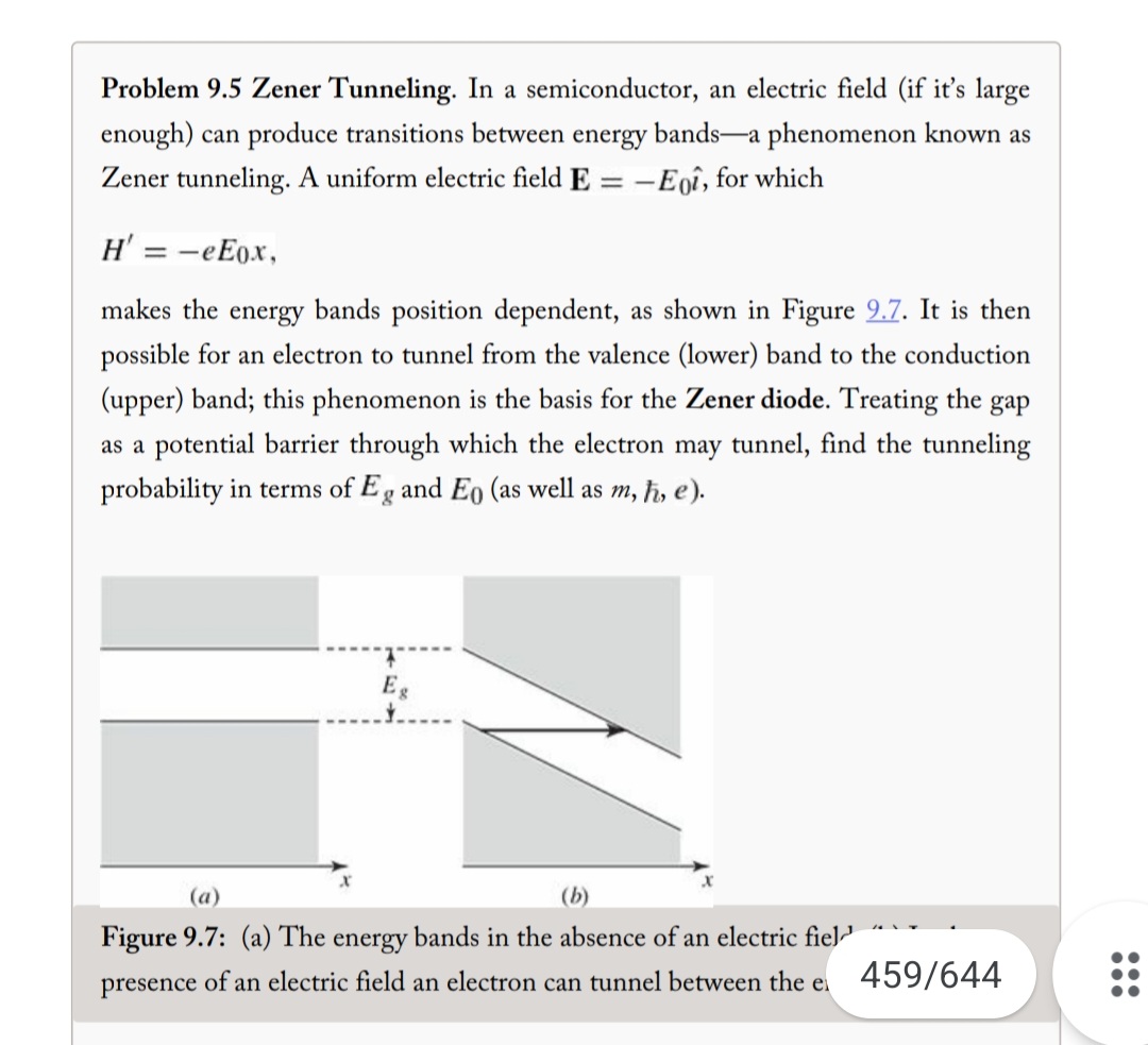

Transcribed Image Text:Problem 9.5 Zener Tunneling. In a semiconductor, an electric field (if it's large
enough) can produce transitions between energy bands-a phenomenon known as
Zener tunneling. A uniform electric field E
=
-Eqî, for which
H' = - eEox,
makes the energy bands position dependent, as shown in Figure 9.7. It is then
possible for an electron to tunnel from the valence (lower) band to the conduction
(upper) band; this phenomenon is the basis for the Zener diode. Treating the gap
as a potential barrier through which the electron may tunnel, find the tunneling
probability in terms of Eg and Eo (as well as m, ħ, e).
X
Eg
(a)
(b)
Figure 9.7: (a) The energy bands in the absence of an electric fiel
presence of an electric field an electron can tunnel between the e
459/644
Expert Solution
This question has been solved!
Explore an expertly crafted, step-by-step solution for a thorough understanding of key concepts.

This is a popular solution

Trending nowThis is a popular solution!

Step by stepSolved in 2 steps with 2 images

Knowledge Booster

Similar questions
- Use the diagram, and your knowledge of how electrons flow, to draw in the expected band-bending of the n-and p-type semiconductors in contact with the metal. Explain what the expected charge distributions will be at the metal-semiconductor junctions.arrow_forwardQ2 part carrow_forward1. In semiconductors, how is conductivityaffected by impurities (doping) and temperature?2. Phosphorous is added to high purity silicon to produce a1023 ?3 charges carrier concentration at room temperature. What is this type of material, n or p?3. Calculate the conductivity of this material at room temperature, assuming that the mobilities of electrons andof the gaps are the same as for the intrinsic material?e = 0.14 and ?h = 0.048 ?/ V s.? = 2240(Ω − ?)-1. P why?arrow_forward