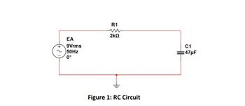
Design and Simulate the circuit in figure 1 using Multisim software and get the following parameters
Current in circuit I =…………………………mA
Voltage across R8 ER =…………………………V
Voltage across C2 EC =…………………………V
Power dissipated P =…………………………mW


Step by stepSolved in 3 steps with 2 images

Compare the values measured in software analysis and calculated in mathematical
analysis and discuss the result obtained.
Draw power triangle of circuit
Draw the phasor diagram of the circuit
Calculate the following values using circuit analysis with detailed steps of calculation.
Reactance of C2 Xc = …………..Ω
Total Impedance ZT = …………..Ω
Current in circuit I =……………mA
Voltage across R8 ER =……………V
Voltage across C2 EC =……………V
Power dissipated P =……………W
Total reactive power in the circuit Q =……………VAr
Apparent power delivered by source S =…………….VA
Observe the following waveforms using oscilloscope
Source voltage and source current waveforms
Voltage across resistor
Voltage across capacitor
- Consider a buck converter with the controlled switch as MOSFET and the uncontrolled switch as diode, the input to buck converter is 60 V. The MOSFET is turned on and off for 20 msec and 10 msec periodically. Assuming ideal components, the output voltage of the buck converter isarrow_forwardThe input voltage of a Boost converter is 10V, the duty cycle of the boost converter is 0.25. If a 10- ohm resistor load is connected to the output; what are the average current flowing in the MOSFET and the diode? what is the max voltage stress on the MOSFET and the diode?arrow_forwardQ9. Draw Zener regulator circuit to obtain regulated DC voltage 6.8 V. Considering input DC voltage in the range from 10V to 30V. Consider load resistance of 110KQ. Q10. Determine maximum and minimum value of Zener current if value of series resistance is 1 K, load resistance is 2KN and input varies from 10V to 30V. Zener voltage is 5 V. Q11. What is LED?arrow_forward
 Introductory Circuit Analysis (13th Edition)Electrical EngineeringISBN:9780133923605Author:Robert L. BoylestadPublisher:PEARSON
 Delmar's Standard Textbook Of ElectricityElectrical EngineeringISBN:9781337900348Author:Stephen L. HermanPublisher:Cengage Learning
 Programmable Logic ControllersElectrical EngineeringISBN:9780073373843Author:Frank D. PetruzellaPublisher:McGraw-Hill Education
 Fundamentals of Electric CircuitsElectrical EngineeringISBN:9780078028229Author:Charles K Alexander, Matthew SadikuPublisher:McGraw-Hill Education
 Electric Circuits. (11th Edition)Electrical EngineeringISBN:9780134746968Author:James W. Nilsson, Susan RiedelPublisher:PEARSON
 Engineering ElectromagneticsElectrical EngineeringISBN:9780078028151Author:Hayt, William H. (william Hart), Jr, BUCK, John A.Publisher:Mcgraw-hill Education,


