For the function F(A,B,C)= (0,2,4,5,6) A. Write the truth table B. By using Karnaugh map find the simple or the simplest expression using POS (product of maxterms) for the given function F. C. Draw the circuit diagram of the expression you found in B by using JUST NAND GATES (You can use NOT itself).


Q: Design a 3 bit ODD Parity generator by performing the following steps Draw its truth table. Derive…
A:
Q: 6. Given the following Boolean function F and the don't care function D as follows: F(A, B, C, D) =…
A: According to the question, Implement the function F together with the don't care function D using…
Q: Obtain sum of products expression for the given NAND network and draw the truth table. Construct the…
A: i) Obtaining sum of product expression for the given NAND gate,
Q: A Boolean function F(A,B,C,D) is described by 2,3,8,10,11,12,14,15.lf using K-map the function is…
A: The K-map of the function can be made as: CD AB C’D’ C’D CD CD’ A’B’ 0 0…
Q: The AND-OR network can be converted to a NAND-NAND network using which theorem? O a. Adsorption O b.…
A:
Q: Simplify the expression given below using K-Map. Also represent the minimized expression using NAND…
A: The given terms are in form of min terms and don't care conditions. The don't care conditions…
Q: ) Logic Function F (x, y, z, w) = ∑ m (0,2,4,6,10,13) + ∑ k (8,12) as sum of minimers is given a)…
A:
Q: A. Half-Adder (H.A) 1. Implement a H.A logic equation for sum and carry using NAND gates only then…
A: Since you have asked multiple questions in a single request, we will be answering only the 1st…
Q: 4. A certain Jose Velarde owns binary slot machine at CASINO FILIPINO. The slot machine is composed…
A: The slot machine has 4 slots which are represented by 4 variables A,B,C and D and the winning of…
Q: 2. Reduce an expression xT +z in forms of NAND operations and draw the final circuit using only NAND…
A: Given expression is F= XY'+Z
Q: Simulate the following Boolean algebra formula Using NAND gate only : Y= A.B.A.B
A: The given Boolean expression can be simulated by using multisim and the actual circuit can be drawn…
Q: 2) A) The simplified Boolean expression for АВС + АвС + АВС + АВС Realize using NAND logic gate…
A: NAND gate- NAND gate is logic circuit whose output is at logic high when any of the input is at…
Q: (a) From the expression X ( (AB*C+(AB)*)*+ABC) where * indicates the complement (i) Draw the logic…
A: A (1): The given expression is: X = (AB'C + (AB)']' + ABC X = (AB'C)' . AB + ABC X = [(AB')' + C']…
Q: Question 1 For the components in the sequential circuit shown below, t is the propagation delay,…
A: Since there are multiple questions uploaded within a single question, so solving the first question…
Q: Given the inputs A,B,C and D please make a truth table for the outputs at points F,G and H (а) U8 A:…
A: Since you have posted the multiple questions so we are supposed to answer the 1st question. a)
Q: Using the simplified Boolean function, draw the actual circuit. Similarly, construct the 3-bit even…
A:
Q: Implement the following Boolean function by using NAND gates only and draw circuit diagram F1…
A: Given Boolean function FA,B,C,D=∑1,2,3,4,7,9,15
Q: Subject Digital Logic Design(DLD) Up Synchronous Counters (0 – 1 – 2 – 3 – 4 – 5 – 6 – 7 – 0)…
A: Types of Counter based on clock Asynchronous Counter The output of the first stage flip flop will…
Q: Develop the truth table for the circuit shown.
A:
Q: A A ↑ B T T F Define the logical operation NAND on propositions A and B, A ↑ B by the truth table: T…
A: It is cleared from the truth table of the NAND operation that the truth value of the compound…
Q: Implement A’C + ABC + BC’D + AB’C using: Frist simplify that and construct truth table and then…
A:
Q: 2. A generic sequential circuit is given below. The circuit's inputs are A, CLK and CLR and output…
A:
Q: Given the following circuit specification, show the truth table, K-Map, and logic diagram:F(w,x,y,z)…
A: Ans. Shown below.
Q: Experiment 5 Simplify the Boolean function below and implement with AND, OR, NOT ICs. F(w,x,y,z) =…
A: The explanation is as follows.
Q: Explain with truth table, symbols and practical applications XOR, NOT, AND gates and also form OR,…
A: (1) X-OR gate Truth-table for 2 input X-OR gate is A B Y=A⊕B 0 0 0 0 1 1 1 0 1 1 1 0…
Q: (b) For the product of maxterm expression Y(A, B, C)=nIM (3, 4, 5, 6, 7), write the Standard POS…
A: To find the standard POS expression
Q: Reduce this boolean equation using the universality of NORs and NANDs LT+L'H+T'H+'PT+'PL+'P'H
A:
Q: Use the Karnaugh diagram to find the minimized SDP of each expression: а) АВС + АBС + АВС + АВС c)…
A:
Q: A combinational circuit is specified by F(A, B, C) = E(1, 4, 6), Implement the circuit with a…
A:
Q: Simplify the following Boolean function F, together with the don't care conditions d, and implement…
A: Given: FA,B,C,D=∑3,6,7,8,10,14,15,dA,B,C,D=∑1,4,5,13. To minimize the given Boolean function, four…
Q: A standard POS expression is given as VA B , C ) NM ( 0,2 , 3 , 6 , 7 ) ( d ) Explain the difference…
A: standard POS expression is given as X(A B , C ) NM ( 0,2 , 3 , 6 , 7 ) A) standard SOP B) Truth…
Q: combinational circuit is specified by F(A, B, C) = › (3,5), Implement the circuit with a decoder…
A: Decoder:It is a combinational circuit which contains n-inputs and 2^n outputs and one enable input.…
Q: 2Design a cirrit of full binary adder using 2-input NAND gates only , and prepare the truth table .
A:
Q: 11. Design a simple circuit from the function by reducing it using appropriate k-map, draw…
A:
Q: Convert boolean expression ABC' + D' to equivalent that uses three NAND gates like in a 7410 chip.…
A: We need to convert the boolean expression to equivalent using only 3 input NAND gates.
Q: A. Simplify: F(ABCD)= E(2,4,6,10,12,14) Perform the truth table Draw the simplified circuit
A:
Q: Q5. For the logical expression given below draw the K-Map and obtain simplified logical expression.…
A:
Q: 10.) Given the following Boolean Algebra representation, generate a MOSFET circuit representation of…
A: F =A B + C Dbut we known that F = F F =F= A B+ C D
Q: EX A combinational Switchinng network, has four inputs La; bocgd) and one out Put CF). The dent is…
A: Given, There are 4 inputs(i.e a,b,c & d) and one output (i.e F). The output F is high(i.e 1) if…
Q: Simplify the following Boolean function F, together with the don't care conditions d, and implement…
A:
Q: 1) (1 ba tare) Draw the R-S latch that is implemented using NAND gates and show its truth table. 2)…
A:
Q: . Simplify the Boolean functionF(A,B,C,D)= ∑ m(0,1,2,3,8,9,10,11,12,13,14,15)using a K-ma. 1b.…
A:
Q: Simplify the following Boolean function F, together with the don't care conditions d, and implement…
A:
Q: Build CMOS circuit using Truth-table method: a) F = a + b + c b) F = abc
A:
Q: Realize the following function using a multilevel NAND-NAND network and NOR-NOR network: F = A′B + B…
A: Given, F = A′B + B (C + D) + EF′ (B′ + D′)
Q: Simplify the following Boolean function F, together with the don't care conditions d, and implement…
A: Note : Since you are asking POS form only so we are providing that without implement the circuit. If…
Q: Q3: A) Express the decimal number (- 30 ) as an 8-bit number in 2's complement form, an verifying…
A:
Q: Which boolean equation
A:
Q: in this exercise you are going to design and build two circuits to give the sum and carry unctions…
A:
Q: la) Simplify the expression using k-map and realize the simplified expression using NAND gates only.…
A: (a) Write the given expression. Draw the K-map for the above expression.
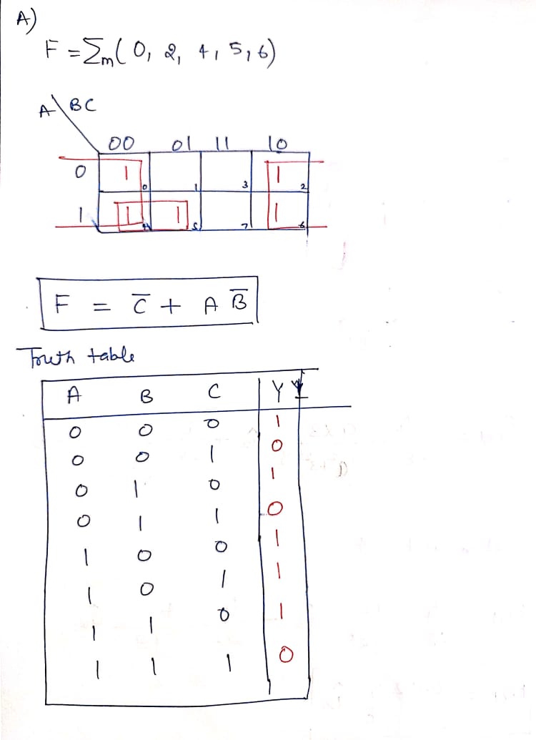
For the function F(A,B,C)= (0,2,4,5,6)
A. Write the truth table
B. By using Karnaugh map find the simple or the simplest
expression using POS (product of maxterms) for the given function F.
C. Draw the circuit diagram of the expression you found in B by
using JUST NAND GATES (You can use NOT itself).
D. Simulate the diagram you found in C, compare the results with
theory & comment on.
.jpg)

Step by step
Solved in 3 steps with 3 images


- Question is below. 1, Draw four-variable Karnaugh Map and find all prime implicants, essential prime implicants. 2,Find simplified Boolean expression for F in SOP form using K-map 3, Implement the simplified Boolean expression using NAND gates only and draw the circuit.- The proportional distribution of A, B, C, D signals is given in the table as a percentage. It “logic 1” when the signals are accepted as active, “logic 0” when they are accepted as passive. takes. - When the proportional sum of active signals is over 50%, its output is "logic1", When we accept "logic 0" when it is below 50%, the output in the table Find the values. - Create an X function based on the logic values you find. Simplify the created X function. - Design the simplified function with NAND and NOR gates. - Set up the circuits you designed with NAND and NOR gates and observe the outputs. Show the output values by drawing a table, applying all possibilities to the input values.- The proportional distribution of A, B, C, D signals is given in the table as a percentage. It “logic 1” when the signals are accepted as active, “logic 0” when they are accepted as passive. takes. - When the proportional sum of active signals is over 50%, its output is "logic1", When we accept "logic 0" when it is below 50%, the output in the table Find the values. - Create an X function based on the logic values you find. Simplify the created X function. - Design the simplified function with NAND and NOR gates.
- An equation in reduced SOP form, is F=AB+B'C+A'C'. I need to draw a logic circuit F using NOT/AND/OR and logoc circuit F using all NAND gates. Thank you for the help. I understood the previous types of gates but I am confused on how to draw these circuits.a) Create a 4 Variable Karnaugh Map in paper by mapping 1’s for given standard SOP Boolean expression. After mapping , make relevant groups within Karnaugh Map by considering rules for making groups for 4 variable Karnaugh Map. After making relevant grouping , extract the minimum SOP expression by considering rules for extracting minimum SOP using Karnaugh Map. * Standard SOP: *Create Circuit Diagram using logic gates and logic converter in Multisim for given standard SOP and minimum SOP which you have solved. Do make sure that truth table for both expressions should evaluate same result.Build frequency dividers, divide-by-2 and divide-by-4 circuit using a. D Flip Flops b. JK Flip Flops You should build 4 circuits in total. D Flip-Flop JK Flip-Flop D Q J Q CLK CLK K Preliminary Work Draw truth tables and logic diagrams of the designs. Construct and test the designed circuits in Quartus II. Equipments D Flip Flop (74LS74). IK Flin Flop (74LS76)
- In this problem we'll explore the fact that all logical circuits can be implemented using just NAND gates. The figure below shows you the symbol for a NAND gate and its truth table. We then show you how NAND gates can be wired together to perform the equivalent of a NOT gate, an AND gate, and an OR gate. NAND gate AB Output 1 01 1 Inputa Inputg Output 10 1 11 NOT A- AND D B. A. OR B. 2 i. Let's denote p NAND q as pīq. Write a logical expression for the thrce circuits corresponding to AND, OR, and NOT. ii. Validate your three logical expressions with three truth tables. For clarity and full credit, show cach variable and distinct sub-clause in a separate column, culminating in your final formula. 3. 2.1. Build an electronic circuit for (A.B)->C a)if you have only electronic gate NAND b)if you have electronic gates TRUE, FALSE, AND,OR,NAND 2. Design the logic diagram for the input and output of F + FA + FB +FC + F(TK)5. Simplify the following function using K-Map and draw logic diagram for that. E(A, B,CD)=Em(0,1,2,3,4,5,7,8,10,11,12,13,14,15)
- so we were asked to implement a 3-bit BCD number on DE0’s board segment display for quartus... using 7447 but 7447 has 4 inputs? (see attached screenshot for problem) also not sure what the items in the second screenshot should be doing? like i can put inputs and outputs..but i don't know what they are? and its not discussed other than they can supply power?a) Using an SR latch and logic gates, design an SN-flipflop which has two input lines (S and N) and two output lines (Q and Q'). The SN-flipflop operates according to the following characteristics table. Determine the characteristics equations and draw circuit diagram of SN-flipflop. Inputs Outputs Q(t+1) Q'(t+1) Q’(t) Q(t) Q(t) Q’(t) Operation S Toggle No-Change 1 1 1 Set 1 1 Q'(t) Q(t) ToggleDigital Electronics and Design QuestionWhich of the following statements in an arbitrary Boolean algebra are correct, which are not?Prove or disprove your claim.(Do not use Karnaugh Map)