Introductory Circuit Analysis (13th Edition)
13th Edition
ISBN: 9780133923605
Author: Robert L. Boylestad
Publisher: PEARSON
expand_more
expand_more
format_list_bulleted
Question
Please explain this with all the steps

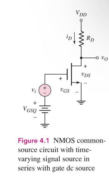
Transcribed Image Text:Vi
VGSQ
+
-
VDD
D
+
VGS
RD
+
VDS
vo
Figure 4.1 NMOS common-
source circuit with time-
varying signal source in
series with gate dc source

Transcribed Image Text:EXERCISE PROBLEM
Ex 4.2: For the circuit shown in Figure 4.1, VDD = 3.3 V and RD = 10 ks. The
transistor parameters are VTN = 0.4 V, k = 100 μA/V², W/L = 50, and
λ= 0.025 V1. Assume the transistor is biased such that IDQ = 0.25 mA. (a) Verify
that the transistor is biased in the saturation region. (b) Determine the small-
signal parameters gm and ro. (c) Determine the small-signal voltage gain.
(Ans. (a) VGsQ = 0.716 V and VDSQ = 0.8 V so that VDS > VDs (sat);
(b) gm 1.58 mA/V, ro = 160 ks2; (c) -14.9)
Expert Solution
This question has been solved!
Explore an expertly crafted, step-by-step solution for a thorough understanding of key concepts.
Step by stepSolved in 2 steps with 6 images

Knowledge Booster
Similar questions
- QUESTION 4 a) Discuss four advantages of field effect transistor (FET) over bipolar junction transistor (BJT). b) With the aid of suitable diagrams, explain the primary difference between n-channel depletion and enhancement type metal oxide semiconductor field effect transistors (MOSFETS).arrow_forwardb. What is the "turn-on" VGs voltage for the N-channel MOSFET transistors?arrow_forward4. Sketch the DC load line for the voltage divider bias circuit for each transistor case and place the Q-point on it. Is there a difference between the load lines in this case?arrow_forward
- State and explain the relation of drain current versus gate to source voltage for an MOSFET.arrow_forwardObjective: Determine the small-signal voltage gain of a circuit biased with a constant- current source and incorporating a source bypass capacitor. +5 V Rp = 7 kn For the circuit shown in Figure 4.21, the transistor parameters are: VTN = 0.8 V, K, = 1 mA/V?, and = 0. o vo RG= 200 k2 +Cs lo = 0.5 mA 4 -5 Varrow_forward
arrow_back_ios
arrow_forward_ios
Recommended textbooks for you
 Introductory Circuit Analysis (13th Edition)Electrical EngineeringISBN:9780133923605Author:Robert L. BoylestadPublisher:PEARSON
 Delmar's Standard Textbook Of ElectricityElectrical EngineeringISBN:9781337900348Author:Stephen L. HermanPublisher:Cengage Learning
 Programmable Logic ControllersElectrical EngineeringISBN:9780073373843Author:Frank D. PetruzellaPublisher:McGraw-Hill Education
 Fundamentals of Electric CircuitsElectrical EngineeringISBN:9780078028229Author:Charles K Alexander, Matthew SadikuPublisher:McGraw-Hill Education
 Electric Circuits. (11th Edition)Electrical EngineeringISBN:9780134746968Author:James W. Nilsson, Susan RiedelPublisher:PEARSON
 Engineering ElectromagneticsElectrical EngineeringISBN:9780078028151Author:Hayt, William H. (william Hart), Jr, BUCK, John A.Publisher:Mcgraw-hill Education,

Introductory Circuit Analysis (13th Edition)
Electrical Engineering
ISBN:9780133923605
Author:Robert L. Boylestad
Publisher:PEARSON

Delmar's Standard Textbook Of Electricity
Electrical Engineering
ISBN:9781337900348
Author:Stephen L. Herman
Publisher:Cengage Learning

Programmable Logic Controllers
Electrical Engineering
ISBN:9780073373843
Author:Frank D. Petruzella
Publisher:McGraw-Hill Education

Fundamentals of Electric Circuits
Electrical Engineering
ISBN:9780078028229
Author:Charles K Alexander, Matthew Sadiku
Publisher:McGraw-Hill Education

Electric Circuits. (11th Edition)
Electrical Engineering
ISBN:9780134746968
Author:James W. Nilsson, Susan Riedel
Publisher:PEARSON

Engineering Electromagnetics
Electrical Engineering
ISBN:9780078028151
Author:Hayt, William H. (william Hart), Jr, BUCK, John A.
Publisher:Mcgraw-hill Education,