
Introductory Circuit Analysis (13th Edition)
13th Edition
ISBN: 9780133923605
Author: Robert L. Boylestad
Publisher: PEARSON
expand_more
expand_more
format_list_bulleted
Related questions
Question
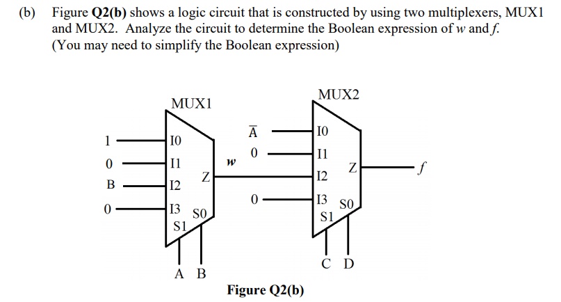

Transcribed Image Text:(b)
Figure Q2(b) shows a logic circuit that is constructed by using two multiplexers, MUX1
and MUX2. Analyze the circuit to determine the Boolean expression of w and f.
(You may need to simplify the Boolean expression)
MUX2
MUX1
I0
1
I0
Il
Il
Z
Z
12
В
12
13
SO
13
SO
Si
si
C D
А В
Figure Q2(b)
Expert Solution
This question has been solved!
Explore an expertly crafted, step-by-step solution for a thorough understanding of key concepts.

Step by stepSolved in 2 steps with 2 images

Knowledge Booster


Learn more about
Need a deep-dive on the concept behind this application? Look no further. Learn more about this topic, electrical-engineering and related others by exploring similar questions and additional content below.Similar questions
- Draw a 4:1 multiplexer using 2:1 multiplexersarrow_forwardSolver 200/5A Is=2.75A Ip=?arrow_forwardIn an AC to DC rectifier circuit, the output DC signal of the rectified wave was measured to be VDc= (7.9±0.8)V and its ripple voltage was measured to be Vripple=(0.38±0.01) mV. What is the uncertainty on the quality factor of the rectifier? Divide your value by 1E-6 and report the answer to 2 decimal places.arrow_forward
- 5. The diagrams a, b and c below show digital pulse trains for three different digital signals. What is the duty-cycle for each signal? b)arrow_forwardasynchronous counters are known as (a) ripple counter (b) multiple clock counters (c) decade counters (d) models countersarrow_forwardIf the frequency of the input signal applied to a full wave rectifier is 120 Hz, then what will be the frequency of the output signal?arrow_forward
- For a half wave or full wave rectifier the Peak Inverse Voltage of the rectifier is always greater than the input voltage. Select one: True O Falsearrow_forwardWhich of the following is most difficult to fabricate in an IC? A. Diode B. Transistor C. FET D. Capacitorarrow_forwardWhat is the period of a 2kHz signal?arrow_forward
arrow_back_ios
arrow_forward_ios
Recommended textbooks for you
- Introductory Circuit Analysis (13th Edition)Electrical EngineeringISBN:9780133923605Author:Robert L. BoylestadPublisher:PEARSON
 Delmar's Standard Textbook Of ElectricityElectrical EngineeringISBN:9781337900348Author:Stephen L. HermanPublisher:Cengage Learning
 Programmable Logic ControllersElectrical EngineeringISBN:9780073373843Author:Frank D. PetruzellaPublisher:McGraw-Hill Education
  Fundamentals of Electric CircuitsElectrical EngineeringISBN:9780078028229Author:Charles K Alexander, Matthew SadikuPublisher:McGraw-Hill Education
 Electric Circuits. (11th Edition)Electrical EngineeringISBN:9780134746968Author:James W. Nilsson, Susan RiedelPublisher:PEARSON
 Engineering ElectromagneticsElectrical EngineeringISBN:9780078028151Author:Hayt, William H. (william Hart), Jr, BUCK, John A.Publisher:Mcgraw-hill Education,
Introductory Circuit Analysis (13th Edition)
Electrical Engineering
ISBN:9780133923605
Author:Robert L. Boylestad
Publisher:PEARSON
Delmar's Standard Textbook Of Electricity
Electrical Engineering
ISBN:9781337900348
Author:Stephen L. Herman
Publisher:Cengage Learning
Programmable Logic Controllers
Electrical Engineering
ISBN:9780073373843
Author:Frank D. Petruzella
Publisher:McGraw-Hill Education
Fundamentals of Electric Circuits
Electrical Engineering
ISBN:9780078028229
Author:Charles K Alexander, Matthew Sadiku
Publisher:McGraw-Hill Education
Electric Circuits. (11th Edition)
Electrical Engineering
ISBN:9780134746968
Author:James W. Nilsson, Susan Riedel
Publisher:PEARSON
Engineering Electromagnetics
Electrical Engineering
ISBN:9780078028151
Author:Hayt, William H. (william Hart), Jr, BUCK, John A.
Publisher:Mcgraw-hill Education,