Introductory Circuit Analysis (13th Edition)
13th Edition
ISBN: 9780133923605
Author: Robert L. Boylestad
Publisher: PEARSON
expand_more
expand_more
format_list_bulleted
Question

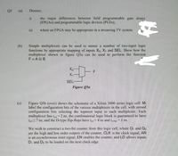
Transcribed Image Text:Q5
(a)
Discuss,
the major dıfferences between ticld programmable gatc arrays
(FPGAS) and programmable logie devices (PLDS.
where an FPGA may be approprate in a streamıng TV system.
Simple multiplexers can be used to mimic a number of two-input logic
functions by appropriate mapping of nputs X X, and SEL Show how the
multiplexer shown in figure Q5a can be used to perform the function
F= AOB
(b)
SEL
Figure Q5a
Figure Q5b (over) shows the schematic of a Xilinx 3000 sennes logic cell M
Label the configuration bits of the various multiplexers n the celL with zeroed
configuration bits selecting the topmost input to each multuplexer. Each
multiplexer has -2 ns, the combinatorial loge block is guaranteed to have
WS7 ns, and the D-type flip-flops have t4 ns and r 1 ns
(c)
We wish to construct a two-bit counter from this logie cell. where Q, and Q
are the high and low order outputs of the counter, CLK is the clock signal, AR
is an asynchronous reset signal, EN enables the counter, and LD allows inputs
D, and Do to be loaded on the next clock edge.
Expert Solution
This question has been solved!
Explore an expertly crafted, step-by-step solution for a thorough understanding of key concepts.
Step by stepSolved in 2 steps with 2 images

Knowledge Booster
Learn more about
Need a deep-dive on the concept behind this application? Look no further. Learn more about this topic, electrical-engineering and related others by exploring similar questions and additional content below.Similar questions
- Which of the following is an important feature of the sum-of-products form of expressions? • The delay times are greatly reduced over other forms. • The maximum number of gates that any signal must pass through is reduced by a factor of two. • No signal must pass through more than 2 gates (not including inverters). • All logic circuits are reduced to nothing more than simple AND and OR gates.arrow_forwardparity generator design, construct and test a circuit that generates an even parity bit ffrom four messages bits . use XOR gates. adding one more XOR gate, expand the circuit so that it generates an odd parity bit also.arrow_forwardDesign a combinational circuit using multiplexer for a car chime based on thefollowing system: A car chime or bell will sound if the output of the logic circuit(X) is set to a logic ‘1’. The chime is to be sounded for either of the followingconditions:• if the headlights are left on when the engine is turned off and• if the engine is off and the key is in the ignition when the door is opened.Use the following input names and nomenclature in the design process:• ‘E’ – Engine. ‘1’ if the engine is ON and ‘0’ if the engine is OFF• ‘L’ – Lights. ‘1’ if the lights are ON and ‘0’ if the lights are OFF• ‘K’ – Key. ‘1’ if the key is in the ignition and ‘0’ if the key is not in the ignition• ‘D’ – Door. ‘1’ the door is open and ‘0’ if the door is closed• ‘X’ – Output to Chime. ‘1’ is chime is ON and ‘0’ if chime is OFFarrow_forward
- Below is an example of an NMOS logic circuit. For all of the MOSFETs in the circuit below, assume V = 1 V and k = 50 mA/V². th W R₂ = 5600 PEETHIPPIN R₁ - 4700 M3 M₁ M. 0 a. Indicate and verify the state of each MOSFET and V for the following input combinations. Fill-out the table below for each assumed state of the MOSFET for every input combination. Use R approximation for linear operation and three significant ds(on) figures for the voltages. 오 Ao SV whyarrow_forwardBy using the information given in image below design a BCD Counter. You have to provide all the necessary information needed to design this circuit.arrow_forwarda) Design a combinational circuit that would take a 3-bit binary number and generate an output if the input value in decimal is either divisible by 2 or 3. iii) Explain and show how you would implement this circuit using a 4-to-1 Multiplexer and other appropriate logic gates. Use a block diagram for the multiplexer.arrow_forward
arrow_back_ios
arrow_forward_ios
Recommended textbooks for you
 Introductory Circuit Analysis (13th Edition)Electrical EngineeringISBN:9780133923605Author:Robert L. BoylestadPublisher:PEARSON
 Delmar's Standard Textbook Of ElectricityElectrical EngineeringISBN:9781337900348Author:Stephen L. HermanPublisher:Cengage Learning
 Programmable Logic ControllersElectrical EngineeringISBN:9780073373843Author:Frank D. PetruzellaPublisher:McGraw-Hill Education
 Fundamentals of Electric CircuitsElectrical EngineeringISBN:9780078028229Author:Charles K Alexander, Matthew SadikuPublisher:McGraw-Hill Education
 Electric Circuits. (11th Edition)Electrical EngineeringISBN:9780134746968Author:James W. Nilsson, Susan RiedelPublisher:PEARSON
 Engineering ElectromagneticsElectrical EngineeringISBN:9780078028151Author:Hayt, William H. (william Hart), Jr, BUCK, John A.Publisher:Mcgraw-hill Education,

Introductory Circuit Analysis (13th Edition)
Electrical Engineering
ISBN:9780133923605
Author:Robert L. Boylestad
Publisher:PEARSON

Delmar's Standard Textbook Of Electricity
Electrical Engineering
ISBN:9781337900348
Author:Stephen L. Herman
Publisher:Cengage Learning

Programmable Logic Controllers
Electrical Engineering
ISBN:9780073373843
Author:Frank D. Petruzella
Publisher:McGraw-Hill Education

Fundamentals of Electric Circuits
Electrical Engineering
ISBN:9780078028229
Author:Charles K Alexander, Matthew Sadiku
Publisher:McGraw-Hill Education

Electric Circuits. (11th Edition)
Electrical Engineering
ISBN:9780134746968
Author:James W. Nilsson, Susan Riedel
Publisher:PEARSON

Engineering Electromagnetics
Electrical Engineering
ISBN:9780078028151
Author:Hayt, William H. (william Hart), Jr, BUCK, John A.
Publisher:Mcgraw-hill Education,