
Introductory Circuit Analysis (13th Edition)
13th Edition
ISBN: 9780133923605
Author: Robert L. Boylestad
Publisher: PEARSON
expand_more
expand_more
format_list_bulleted
Related questions
Question
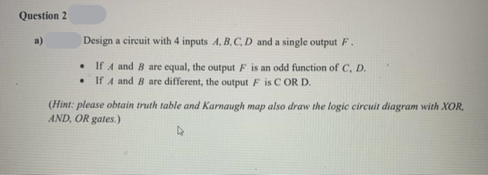

Transcribed Image Text:Question 2
a)
Design a circuit with 4 inputs A, B, C, D and a single output F.
• If A and B are equal, the output F is an odd function of C, D.
If A and B are different, the output F is C OR D.
(Hint: please obtain truth table and Karnaugh map also draw the logic circuit diagram with XOR,
AND, OR gates.)
Expert Solution
This question has been solved!
Explore an expertly crafted, step-by-step solution for a thorough understanding of key concepts.

Step by stepSolved in 3 steps with 3 images

Knowledge Booster


Learn more about
Need a deep-dive on the concept behind this application? Look no further. Learn more about this topic, electrical-engineering and related others by exploring similar questions and additional content below.Similar questions
- hi, i have a problem with this logic gate question. can you please help me.arrow_forwardThe source impedance Z, = (12 + j5) Q in the circuit shown (Fig. 2). Maximum power is transferred to the load impedance when Z, is equal to Fig.2arrow_forward(b) For the following circuits, (i) Write down the logic statement (ii) write down the truth table Aarrow_forward
- Q) You want to design a synchronous counter sequential (sequential) logic circuit. Counting from 0 to 9 and will not count the last two digit of your student number. (a) List the steps that you will apply in the design approach. State Chart and State Create the table. (b) Design the sequential circuit using JK Flip-Flop. Explain each step. Desired action show that you have done it. " last two digit student num: 0 4 " Not : I want the solution to contain tables and equations, and the electrical circuit resulting from tables and equations, as in the picture that I attached,And if possible, I want the solution on paper if possible.arrow_forwardDraw in Table 3 the circuit schematic of each segment using the basic logic gates in kmaparrow_forwardReduce the Boolean function specified in the truth table below to its minimum SOP form using K-map, where A, B, C are the inputs while X are the outputs. Based on the reduced Boolean function, design the logic circuit using any logic gates. A 0 0 0 0 1 1 1 1 B 0 0 1 1 0 1 с 0 1 0 1 0 1 0 1 X 1 1 0 1 1 1 0 1arrow_forward
- LOGIC GATE ( NEED ONLY HANDWRITTEN SOLUTION PLEASE OTHERWISE DOWNVOTE).arrow_forwardPLease Explain the design process of this thoroughlyarrow_forwardwhat is the relation bet are the relations be Carry Out outputs of figures in step 3 and step 4? What is the relation between inputs & the sum output in half adder? What is the purpose of half adder and full adder logic circuits? fullarrow_forward
arrow_back_ios
arrow_forward_ios
Recommended textbooks for you
- Introductory Circuit Analysis (13th Edition)Electrical EngineeringISBN:9780133923605Author:Robert L. BoylestadPublisher:PEARSON
 Delmar's Standard Textbook Of ElectricityElectrical EngineeringISBN:9781337900348Author:Stephen L. HermanPublisher:Cengage Learning
 Programmable Logic ControllersElectrical EngineeringISBN:9780073373843Author:Frank D. PetruzellaPublisher:McGraw-Hill Education
  Fundamentals of Electric CircuitsElectrical EngineeringISBN:9780078028229Author:Charles K Alexander, Matthew SadikuPublisher:McGraw-Hill Education
 Electric Circuits. (11th Edition)Electrical EngineeringISBN:9780134746968Author:James W. Nilsson, Susan RiedelPublisher:PEARSON
 Engineering ElectromagneticsElectrical EngineeringISBN:9780078028151Author:Hayt, William H. (william Hart), Jr, BUCK, John A.Publisher:Mcgraw-hill Education,
Introductory Circuit Analysis (13th Edition)
Electrical Engineering
ISBN:9780133923605
Author:Robert L. Boylestad
Publisher:PEARSON
Delmar's Standard Textbook Of Electricity
Electrical Engineering
ISBN:9781337900348
Author:Stephen L. Herman
Publisher:Cengage Learning
Programmable Logic Controllers
Electrical Engineering
ISBN:9780073373843
Author:Frank D. Petruzella
Publisher:McGraw-Hill Education
Fundamentals of Electric Circuits
Electrical Engineering
ISBN:9780078028229
Author:Charles K Alexander, Matthew Sadiku
Publisher:McGraw-Hill Education
Electric Circuits. (11th Edition)
Electrical Engineering
ISBN:9780134746968
Author:James W. Nilsson, Susan Riedel
Publisher:PEARSON
Engineering Electromagnetics
Electrical Engineering
ISBN:9780078028151
Author:Hayt, William H. (william Hart), Jr, BUCK, John A.
Publisher:Mcgraw-hill Education,