Introductory Circuit Analysis (13th Edition)
13th Edition
ISBN: 9780133923605
Author: Robert L. Boylestad
Publisher: PEARSON
expand_more
expand_more
format_list_bulleted
Concept explainers
Question

Transcribed Image Text:TEST
Read the question carefully. Write the letter for each correct answer in the blank space
provided.
A
1. Maximum power is delivered from a source of power to a load when
the
a. load current is equal to the power source current
b. impedance of the load is equal to the output impedance of the power
source
c. output impedance of the power source is high compared to the
impedance of the load
d. output impedance of the power source is low compared to the
impedance of the load
2. The emitter follower is a (an)
a. impedance matching device
b. high gain voltage amplifier
c. phase inverter
d. combination power and voltage amplifier
3. The emitter follower uses
a. no collector resistor
b. a forward bias collector-base junction
c. negative feedback (degeneration)
d. an NPN transistor only
4. The emitter follower has
output resistance.
a. high, high
b. low, low
c. low, high
d. high, low
input resistance and
5. The current gain of an emitter follower is
a. less than 1
b. equal to 1
c. greater than 1
d. less than a common amplifier

Transcribed Image Text:3-12
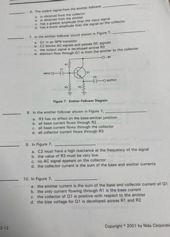
6. The output signal from the emitter follower.
a. is obtained from the collector
b. is obtained from the emitter
c. has a greater amplitude than the input signal
d. has a lower amplitude than the signal on the collector
7. In the emitter follower circuit shown in Figure 7.
a. Q1 in an NPN transistor
b. C2 blocks AC signals and passes DC signals
c. the output signal is developed across R3
d. electron flow through Q1 is from the emitter to the collector
O-9
Q
www.
2
with
01
C2
HTO OUTPUT
Figure 7. Emitter Follower Diagram
8. In the emitter follower shown in Figure 7,
a. R3 has no effect on the base-emitter junction
b. all base current flows through R2
c. all base current flows through the collector
d. all collector current flows through R3
9. In Figure 7,
a. C2 must have a high reactance at the frequency of the signal
b. the value of R3 must be very low
c. no AC signal appears on the collector
d. the collector current is the sum of the base and emitter currents
10. In Figure 7,
a. the emitter current is the sum of the base and collector current of Q1
b. the only current flowing through R1 is the base current
c. the collector of Q1 is positive with respect to the emitter
d. the bias voltage for Q1 is developed across R1 and R2
Copyright 2001 by Nida Corporati
Expert Solution
This question has been solved!
Explore an expertly crafted, step-by-step solution for a thorough understanding of key concepts.
Step by stepSolved in 2 steps with 1 images

Knowledge Booster
Learn more about
Need a deep-dive on the concept behind this application? Look no further. Learn more about this topic, electrical-engineering and related others by exploring similar questions and additional content below.Similar questions
- Question 2 (a) To achieve correct operation when using a Bipolar Transistor how should the two p-n junctions be biased?arrow_forwardMeasurements taken with an E-MOSFET indicate that when VGS=+4V, ID=8mA, and when VGS=+6V, ID=32mA. Determine the value of k.arrow_forwardVec +12V Re 1kS2 Re 470k2 BC107 Vc Ve Figure 3: Practical Fixed Bias Transistor Circuit 2. Measure the DC voltages Vc and VB using digital multi-meters. Determine the quiescent base current, collector current, and collector- emitter voltage.arrow_forward
- 2. Differentiate between forward biasing and reverse biasing of PN Junction.arrow_forwardElectronics for electricians explain the relationship between Base-emitter current and Collect-emitter current.arrow_forwardchoose the correct answer 1-The output voltage of an emitter follower isa-In phase with Vin . b-Much greater than Vin . c-180° out of phase.d-Generally much less than Vin .2-The ac emitter resistance of an emitter followera-Equal the dc emitter resistance .b-Is larger than the load resistance .c-Is β times smaller than the load resistance. d-Is usually less than the load resistance.3-A common-base amplifier can be used when a-Matching low to high impedance.b-A voltage gain without a current gain is required. c-A high- frequency amplifier is needed.d-All of the above.arrow_forward
- (a) What is the output current IO in the circuitshown if −VEE = −10 V andR = 20 ohm? Assume that the MOSFET is saturated.(b) What is the minimum voltage VDDneeded to saturate the MOSFET if VTN = 2.5 Vand K'n = 0.25 A/V2. (c) What must be the powerdissipation ratings of resistor R and the FET.arrow_forwardDetermine thel 1.V B, c and V for the transistor circuit in Figure. Rc 430 Q Rg Vcc A) Poc = 50 24 V 4.7 ko VBB 2 Varrow_forwardPlease show workarrow_forward
arrow_back_ios
SEE MORE QUESTIONS
arrow_forward_ios
Recommended textbooks for you
 Introductory Circuit Analysis (13th Edition)Electrical EngineeringISBN:9780133923605Author:Robert L. BoylestadPublisher:PEARSON
 Delmar's Standard Textbook Of ElectricityElectrical EngineeringISBN:9781337900348Author:Stephen L. HermanPublisher:Cengage Learning
 Programmable Logic ControllersElectrical EngineeringISBN:9780073373843Author:Frank D. PetruzellaPublisher:McGraw-Hill Education
 Fundamentals of Electric CircuitsElectrical EngineeringISBN:9780078028229Author:Charles K Alexander, Matthew SadikuPublisher:McGraw-Hill Education
 Electric Circuits. (11th Edition)Electrical EngineeringISBN:9780134746968Author:James W. Nilsson, Susan RiedelPublisher:PEARSON
 Engineering ElectromagneticsElectrical EngineeringISBN:9780078028151Author:Hayt, William H. (william Hart), Jr, BUCK, John A.Publisher:Mcgraw-hill Education,

Introductory Circuit Analysis (13th Edition)
Electrical Engineering
ISBN:9780133923605
Author:Robert L. Boylestad
Publisher:PEARSON

Delmar's Standard Textbook Of Electricity
Electrical Engineering
ISBN:9781337900348
Author:Stephen L. Herman
Publisher:Cengage Learning

Programmable Logic Controllers
Electrical Engineering
ISBN:9780073373843
Author:Frank D. Petruzella
Publisher:McGraw-Hill Education

Fundamentals of Electric Circuits
Electrical Engineering
ISBN:9780078028229
Author:Charles K Alexander, Matthew Sadiku
Publisher:McGraw-Hill Education

Electric Circuits. (11th Edition)
Electrical Engineering
ISBN:9780134746968
Author:James W. Nilsson, Susan Riedel
Publisher:PEARSON

Engineering Electromagnetics
Electrical Engineering
ISBN:9780078028151
Author:Hayt, William H. (william Hart), Jr, BUCK, John A.
Publisher:Mcgraw-hill Education,