
Introductory Circuit Analysis (13th Edition)
13th Edition
ISBN: 9780133923605
Author: Robert L. Boylestad
Publisher: PEARSON
expand_more
expand_more
format_list_bulleted
Related questions
Question
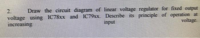

Transcribed Image Text:2.
Draw the circuit diagram of linear voltage regulator for fixed output
voltage using IC78xx and IC79xx. Describe its principle of operation at
input
voltage.
increasing
Expert Solution
This question has been solved!
Explore an expertly crafted, step-by-step solution for a thorough understanding of key concepts.

Step by stepSolved in 3 steps with 3 images

Knowledge Booster


Learn more about
Need a deep-dive on the concept behind this application? Look no further. Learn more about this topic, electrical-engineering and related others by exploring similar questions and additional content below.Similar questions
- Design of a DC-DC Converter. The Circuit Below shows a basic Buck-Boost Converter with a highly inductive Load. With a Deliberate mistake in the configuration of the Circuit Connection. The Value of L1 is 22mH, C1 is 10uF, R1 is 220 and L2 is 10mH. The circuit operates with a switching frequency of 20KHZ. The Duty cycle of the Clock signal V2 is given by the function below: ( 17 ) х0.2 Duty Cycle, k = 0. 55 + 100 Your Unique Duty Cycle = %3D Buck-Boost Converter Q1 IRG4BC10U D1 R1 222 1N4009 C1 LV1 12V L1 22mH 10µF L2 10mH a) Find the mistake in the configuration of the circuit and correct the connection error.arrow_forwardDesign a CT-FWR to supply a load of (50) with a waveform of the following specifications: - Vdc = 12 V Ripple factor = 0.1 % the main power supply is (220 Vrms, 50 Hz). Determine the following values: - 1- The value of capacitor filter. 2- The maximum load voltage (VmR) 3- The transformer turns ratio (a). 4- The RMS value of the load voltage. 5- Draw the output waveform. (assume ideal diodes)arrow_forwardHello. I am curious why does the MOSFET i -v characteristic "flatten out" in the saturatin region?arrow_forward
- QUESTION 1 Design a high efficiency 3.3 V, 5A d.c.to d.c. power converter from a 4 to 5.5 Vdc source. The maximum allowable inductor current ripple and output voltage ripple are 0.1A and 20 mV, respectively. Assume a switching frequency of 20 kHz. a) Design a suitable converter power circuit using a MOSFET switch, showing all calculation of inductor and capacitor values and drawing a circuit diagram of the final design including component values. Indicate the peak inverse voltage and forward current rating of any diode required, and the maximum drain- source voltage of the MOSFET. b) On the Schematic diagram, draw the path of the current flow during the ON time and the OFF time. c) Describe the effect of changing the values of the inductor and the capacitor in the circuit. d) What is the effect of switching frequency in the circuit? e) Draw the schematic diagram of a circuit with the output voltage higher than the input voltage.arrow_forwardIDSS=8mA , VP =-4VTo help plot the DC load line VGS=VG-IDRSa)Attach a Plot of JFET Characteristic Curve as shown in Figureb)What is the approximate VGSQ?c)What is the approximate IDQ in mA?d)Determine source voltage VS.e)Calculate the drain voltage VD.f)Calculate the drain-to-source voltage VDS.arrow_forwardAn ac LVDT has the following data; input 6.3V, output 5.2V, range ±0.50 cm. Determine: a) Plot of output voltage versus core position for a core movement going from +0.45cm to -0.03cm? b) The output voltage when the core is -0.35cm from the center? c) The core movement from center when the output voltage is -3V? d) The plot of core position versus output voltages varying from +4V to -2.5V.arrow_forward
- Q2) Design a Bridge FWR to supply a load of (1002) with the waveform shown in figure from the main power supply of (220 Vrms). Find: - 1- The transformer turns ratio (a). 2- The ripple voltage. Vot Vm = 12 V 3- The Vde value. 4- The RMS value of the output voltage. 5- The ripple factor. 6- The value of capacitor filter. Vip = 0.1 V (assume ideal diodes) T=0.01 sec. tisec) Q3) V in Design a regulated circuit to supply a constant voltage of (10 V) across a resistive load of (50 2). The input voltage is shown in the figure. The minimum current for the Zener diode operation is (Izk=5mA). Find the 15 V 15 maximum power dissipated in the Zener diode. 12.5 12 V 10arrow_forwardAnálisis de rectificador onda completa Consider the capacitor-filter rectifier circuit as shown in Figure 1. The input is a single-phase source that is derived from a 220 Vrms mains. Tasks for analysis: (a) Rig up the circuit as shown in Figure land plot V andi versus time. (b) Why is there ringing on the current wave-form? (c) What is the series impedance of the circuitệ (d) Plot V and V. versus time. What is the ripple? How does ripple depend on load, capacitor C; and frequency of input wave-form? (e) Measure the current and voltage waveform across the rectifier diode. (f) Estimate the average and ms currents through the rectifier diode, Calculate the diode power dissipation. (g) What should be the peak current rating of the diode? (h) Change the initial charge voltage on the capacitor Cr. What is the effect on the input surge current? (i) Change the phase angle of the input V, at start up. Observe the effect on current i. What happens and why? 1) Under whaf conditions do you get…arrow_forward3 A peak rectifier (peak tollower) Cir cuit is gian below. Vs is a GOH3 Sinuscidal Vollge with peak value Upz50V. 50V. The load resistance R= Sk . Find the Vallke of the capacitance C Such that the peak- to-peak ripple 2 volts. (idenl diede) Voltage Vr Vsarrow_forward
- Q3) A. A step down de chopper is connected to an R=52 and L=10 mH. The de supply voltage is 100 V. The chopper is switching at a frequency of 1 kHz with a duty cycle of 50%. Determine the load current, lo and the peak to peak ripple current as an absolute value and as percentage of de value.arrow_forwardExplain the concept of power semiconductor devices such as Insulated Gate Bipolar Transistors (IGBTs) and Thyristors. How do these devices enable efficient power control and switching in high-power applications?arrow_forwardIdeally, a dc load line is a straight line drawn on the collector characteristic curves between VCE(cutoff) and /C(sat) the Q-point and cutoff the Q-point and saturation IB = 0 and IB = IC / Bdcarrow_forward
arrow_back_ios
SEE MORE QUESTIONS
arrow_forward_ios
Recommended textbooks for you
- Introductory Circuit Analysis (13th Edition)Electrical EngineeringISBN:9780133923605Author:Robert L. BoylestadPublisher:PEARSON
 Delmar's Standard Textbook Of ElectricityElectrical EngineeringISBN:9781337900348Author:Stephen L. HermanPublisher:Cengage Learning
 Programmable Logic ControllersElectrical EngineeringISBN:9780073373843Author:Frank D. PetruzellaPublisher:McGraw-Hill Education
  Fundamentals of Electric CircuitsElectrical EngineeringISBN:9780078028229Author:Charles K Alexander, Matthew SadikuPublisher:McGraw-Hill Education
 Electric Circuits. (11th Edition)Electrical EngineeringISBN:9780134746968Author:James W. Nilsson, Susan RiedelPublisher:PEARSON
 Engineering ElectromagneticsElectrical EngineeringISBN:9780078028151Author:Hayt, William H. (william Hart), Jr, BUCK, John A.Publisher:Mcgraw-hill Education,
Introductory Circuit Analysis (13th Edition)
Electrical Engineering
ISBN:9780133923605
Author:Robert L. Boylestad
Publisher:PEARSON
Delmar's Standard Textbook Of Electricity
Electrical Engineering
ISBN:9781337900348
Author:Stephen L. Herman
Publisher:Cengage Learning
Programmable Logic Controllers
Electrical Engineering
ISBN:9780073373843
Author:Frank D. Petruzella
Publisher:McGraw-Hill Education
Fundamentals of Electric Circuits
Electrical Engineering
ISBN:9780078028229
Author:Charles K Alexander, Matthew Sadiku
Publisher:McGraw-Hill Education
Electric Circuits. (11th Edition)
Electrical Engineering
ISBN:9780134746968
Author:James W. Nilsson, Susan Riedel
Publisher:PEARSON
Engineering Electromagnetics
Electrical Engineering
ISBN:9780078028151
Author:Hayt, William H. (william Hart), Jr, BUCK, John A.
Publisher:Mcgraw-hill Education,