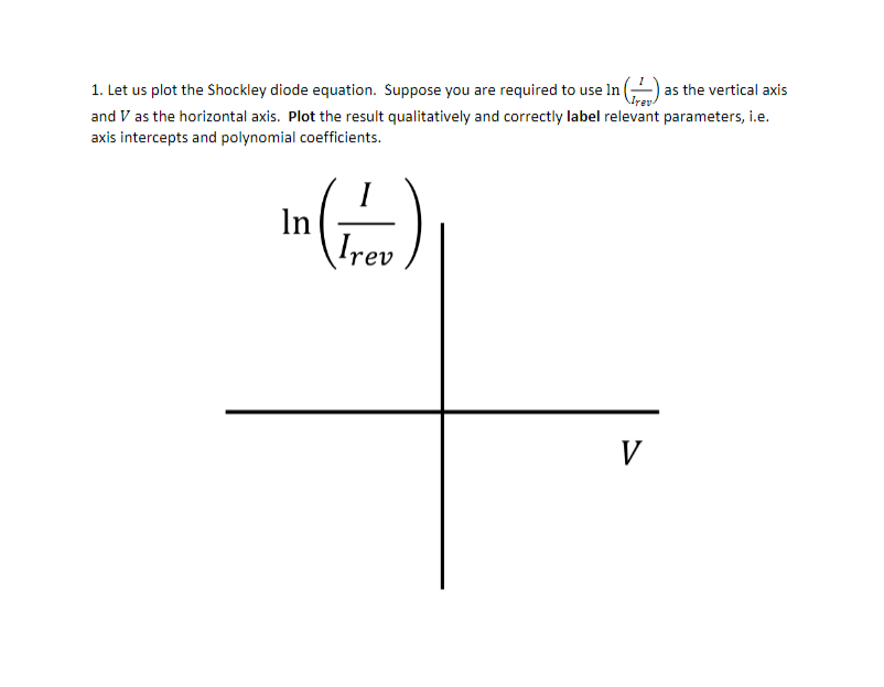
1. Let us plot the Shockley diode equation. Suppose you are required to use In () as the vertical axis and V as the horizontal axis. Plot the result qualitatively and correctly label relevant parameters, i.e. axis intercepts and polynomial coefficients. In Irev V
Q: Describe in your own words the characteristics of the ideal diode and how they determine the on and…
A: What is an ideal diode? When voltage is applied forward biased, an ideal diode works as a perfect…
Q: Plot the diode forward characteristics from the results obtained, and determine the cut in voltage…
A: The given data are:
Q: 1- We start considering the forbidden gap when the lattice spacing is nm. 2- What is the transient…
A: As per our company guidelines we are supposed to answer only first 3 sub-parts. Kindly repost other…
Q: Plot the characteristic curve of the zener diode in the reverse-breakdown region from the results…
A: Zener didoe works as voltage regulator in reverse breakdown region
Q: What is the small-signal diode resistance rd at room temperature for ID = 1.5 mA? What is the…
A: Given Diode current, Id =1.5 mA Temperature, T=100 C The small signal diode resistance of a diode is…
Q: Consider an ideal, silicon PN junction diode with uniform cross section and constant  
A: (a)The built in voltage can be calculated as, Substituting the given values in the above equation,…
Q: For the values of R1=230, R2=230, R3=400, Vs=15. If the real diode (offset voltage=0.7V) were…
A: According to question: As it is given that diode is conducting, so the diode will be replaced by a…
Q: ind the current-voltage relationship of the assumed circuit shown assuming both diodes are Germanium…
A:
Q: How much is the barrier potential, VB, for a; a. germanium diode? b. silicon diode? In a diode, what…
A: Barrier potential of germanium diode is 0.3V Barrier potential of silicon diode is 0.7V
Q: Explain the construction and working of the PN junction diode, with characteristics curve
A: Construction The PN junction diode consists of a p-type semiconductor layer and an n-type…
Q: breakdown
A: The zener diode is a semiconductor device which allow flow of current in both forward and backward…
Q: For the zener regulator circuit given below, zener diode breakdown voltage is given as Vz=10V, (you…
A:
Q: The npn transistor is connected in an alternate“diode” configuration. Use the transport model…
A:
Q: How can we measure the impurity -1 ?concentration The average thermal velocity of electrons at -2…
A: The impurities are added to a pure semiconductor to increase the electrical conductivity.A pure…
Q: For the circuit shown in the Figure, consider Ideal diode. If Vin:
A: In this question , we will find maximum output voltage ...
Q: Q4. In the full-wave diode rectifier shown below, the diodes are ideal. The source voltage is v, =…
A:
Q: Q6. Can we operate normal PN junction diode in breakdown region for longer duration? Give reason Q7.…
A: Ans. 6 No, we can't operate normal PN junction diode in breakdown region for longer duration. Since,…
Q: From the circuit shown in the figure below determine the following: 1. How much load current is…
A:
Q: Given the clamper circuit below, assume that the value of R and C are large enough so the voltage…
A:
Q: 5. Suppose we are given a pn diode, and we apply the applied voltage Vapp to the n-type and ground…
A: The diode circuit can be drawn as:
Q: Give a design for a pn diode voltage reference source that outputs 5 volts DC from a 12-volt source.…
A: Stack of 7 diodes: If V0 is 5V and all diodes are equal, then the voltage drop on the diodes will…
Q: A With diagram, explain the effect of reverse bias on the depletion region. Find the power delivered…
A: (A) The below diagram shows a diode with reverse bias condition, In reverse bias, a negative…
Q: Examine the circuits shown below for each half cycle. On each circuit indicate clearly which diode…
A: Since you have posted a question with multiple sub-parts, we will solve the first three sub-parts…
Q: Kindly explain it to me this question below. No need to illustrate just explain directly. Draw the…
A: Diode: It is a semiconductor device that is on in the forward bias condition and off in the reverse…
Q: 5. Suppose we are given a pn diode, and we apply the applied voltage Va to the n-type and ground the…
A: Generally, the characteristics of p-n junction diode is, This characteristics is obtained when p is…
Q: 1. Plot the characteristic curve of the zener diode in the reverse-breakdown region from the results…
A:
Q: What is the difference between Ideal, Silicon and Germanium diodes in term of forward and reverse…
A: For forward biased voltage . For ideal diode there was no voltage drop that is that will turn on…
Q: Si 12 V
A:
Q: For a silicon pn junction under forward biased condition, the reverse saturation current is 10 nA.…
A: Using Shockley’s equation, the value of the current flowing through a p-n junction diode can be…
Q: From the data collected in Tables 1 and , plot the current versus voltage characteristic of the…
A: The voltage-current characteristics plot is a basic graphical representation to study any circuit…
Q: Make a sketch of the I–V characteristic curve for a diode with Is = 0.02 pA for VD values from zero…
A: According to the question we have to Make a sketch of the I–V characteristic curve and find is the…
Q: 1- We start considering the forbidden gap when the lattice spacing is nm. 2- What is the transient…
A: As per our guidelines we are supposed to answer only one question. Kindly repost other questions as…
Q: In each of the ideal-diode circuits shown below V1 is a 1kHz, 10-V peak sine wave. Sketch the…
A: The diode circuits shown below V1 is a 1kHz, 10-V peak sine wave. its positive and negative peak…
Q: Describe in your own words the characteristics of the ideal diode and how they determine the on and…
A:
Q: What should be the value of Vi, if we have a Zener Diode with a breakdown voltage of 6.2 volts and a…
A:
Q: 3 Determine the labelled voltage and currents if V1 = 10 V and V2 = 5 V. Assume diode cut-in voltage…
A: Given data, V1=10 V, V2=5 V Internal resistance of diode, RD=0.1 kΩ Cut in voltage of diode VD=0.3 V
Q: 1) Describe in your own words the characteristics of the ideal diode and how they determine the on…
A: 1) The ideal diode characteristics are given below, When forward biased, the ideal diode offers…
Q: Consider the diode circuit shown below. If in the given circuit, Vs is replaced by a 12V battery…
A: Diode starts conducting when anode voltage is greater than cathode voltage and ideal diode maintains…
Q: Answer the following. Use a detailed explanation. 1.What diode approximation has a voltage drop and…
A:
Q: 1. Explain dc diode resistance and ac diode resistance in terms of definitions, formula, and…
A: Since there are multiple questions uploaded within the same question, therefore solving 1st question…
Q: Using constant-voltage diode model, where VDO = 0.5 V, plot vo versus vi. Make sure to show all…
A:
Q: From the approximate diode characteristic equation, derive an expression for the dynamic resistance…
A:
Q: If the n-type Ge is brought into contact with p-type Ge to form a pn junction, sketch the band…
A: We need to draw to energy band diagram for given Ge diode .
Q: (a) Find the percentage ripple across the load resistamce Rya (h) Derive the expressions oft the…
A: In the below given rectifier circuit we have two diodes which are connected with capaciter 100μF and…
Q: i. A silicon sample is uniformly doped p-type with Na=1015/cm³. At T=0 K, what are the equilibrium…
A: Given data:
Q: Draw the equivalent circuit and characteristic curve of a forward biased diode using the second or…
A: In this question, We need to determine the Draw the equivalent circuit. The characteristic curve of…
I_rev is the reverse bias current, also labe the appropriate spot on the IV plot with the parameter name I_rev. Please show all work and thank you
Trending now
This is a popular solution!
Step by step
Solved in 2 steps
- Sketch i against v to scale for the circuit. The diodes are typycal small-signal silicon devices 300 K. The reverse-breakdown voltages of the diodes are shown. Assume .6 V for all diodes (including Zenners) in the forward-bias region.True or False. Please explain. thank you As the temperature increases, the forward voltage decreases in a silicon diode. Then, the graph of the forward bias region will shift to the left.Given the clamper circuit below, assume that the value of R and C are large enough sothe voltage across the capacitor does not change significantly during the interval of time.a. Using the simplified diode model, simulate the action of the circuit when the Silicon diode isin forward and reverse bias condition and measure the corresponding output voltage.b. Draw the complete output waveform of the circuit
- For the circuit shown below, compute the maximum current through each resistor when terminal A is a) positive and, b) negative. Assume the diodes are ideal. (Will we convert to the RMS value to it's actual value?)Assuming that the diodes are ideal, determine whether each diode is ON (short circuit) or OFF (open circuit) and find the quantities indicated as V and I on the circuits below. Show guesses and verification work.Two identical Schottky diodes are connected in series, one in the forward and the other in reverse direction, see figure. Assume the reverse saturation current, IS, of each diode to be known. Derive he current-voltage curve I(V) of this circuit. Plot it with the ratio I / IS on the y-axis and V / Vth on the x-axis. Make sure to cover a broad range of voltages, say, from –10 Vth to 10 Vth.
- Determine the current I in the circuit (i). Assume the diodes to be of silicon and forward resistance of diodes to be zero.Consider the circuit with three diodes and a AC input, as shown below: D2 R1 D1 D3 R2 Assume that the input AC voltage is Ttsin(100TTT). You may consider the diodes to be ideal. mean voltage generated across resistor R2 is (assuming current direction to be from AC so into R1, through diode network, and through R2 from top to bottom): O a. 0.5V Ob. -0.5V O c. 1V O d. OVDetermine the forward voltage, forward current, and the voltage across the diode in the Figure below, assuming an ideal diode.
- Determine the small signal resistance of the diode by assuming a constant voltage drop model for the diode. Assume that the thermal voltage is 25mV.Suppose we have a 10-V-peak sinusoidal voltage source. Draw the diagram of a circuit that clips off the part of the sinusoid above 5 V and below -4 V. The circuit should be composed of ideal diodes, dc voltage sources, and other components as needed. Be sure to label the terminals across which the clipped output waveform vo(t) appears.Consider the following circuit diagram. Using practical diode model solve the following items. i. What is the type of rectification in this circuit? ii. Calculate the total peak secondary voltage (Note that “RMS" value is given in the circuit) iii. Sketch the plot of time vs voltage over Load (RL) iv. Find the average voltage over Load. v. Find the maximum current passing over diodes. vi. Find the peak inverse voltage (PIV) over the diodes. vii. Find the minimum fuse current rating for the primary coil. 5:1 D DA 120 V rms D3 D2 RL=10kQ RL out ell lelll