Vcc = 12 V Rc 4.3 kQ 30 k2 Ст R 0.1 μFR vo Thévenin 1 k2 100 k2 2 μΕ transformation R1 R1 RE C3 10 k2 1 k2 RB R 4.12 k2 1.3 k2 10 μF 7.5 k2 (a) (b) Figure 17.34 (a) Common-emitter amplifier. (b) High-frequency ac model for amplifier in (a).
Vcc = 12 V Rc 4.3 kQ 30 k2 Ст R 0.1 μFR vo Thévenin 1 k2 100 k2 2 μΕ transformation R1 R1 RE C3 10 k2 1 k2 RB R 4.12 k2 1.3 k2 10 μF 7.5 k2 (a) (b) Figure 17.34 (a) Common-emitter amplifier. (b) High-frequency ac model for amplifier in (a).

Introductory Circuit Analysis (13th Edition)
13th Edition
ISBN:9780133923605
Author:Robert L. Boylestad
Publisher:Robert L. Boylestad
Chapter1: Introduction
Section: Chapter Questions
Problem 1P: Visit your local library (at school or home) and describe the extent to which it provides literature...

Related questions
Question
Find the midband gain and the frequencies of the poles and zeros of the commonemitter amplifier as shown if the transistor has fT = 500 MHz, but Cμ = 1 pF.

Transcribed Image Text:Vcc = 12 V
Rc
4.3 kQ
30 k2
Ст
R
0.1 μFR
vo
Thévenin
1 k2
100 k2
2 μΕ
transformation
R1
R1
RE
C3
10 k2
1 k2
RB
R
4.12 k2
1.3 k2
10 μF
7.5 k2
(a)
(b)
Figure 17.34 (a) Common-emitter amplifier. (b) High-frequency ac model for amplifier in (a).
Expert Solution
Step 1
Given fT = 500 MHz, Cµ = 1 pF, ID = 0.2 mA, VDS = 5 V
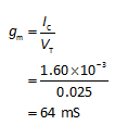
Calculating transconductance of the transistor
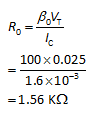
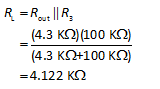
Calculating small signal resistance R0
Step 2
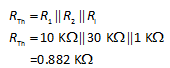
Calculating RTh
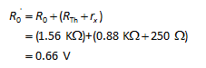
Calculating small signal input resistance R0’
Calculating load resistance
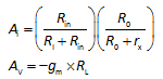
Step 3
Calculating input stage gain and terminal voltage gain in the below expression
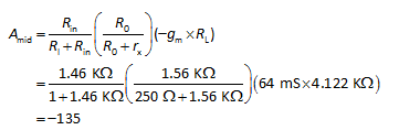
Calculating mid band gain

Substituting value of input stage gain and voltage gain in the above expression

Step by step
Solved in 6 steps with 13 images

Knowledge Booster


Learn more about
Need a deep-dive on the concept behind this application? Look no further. Learn more about this topic, electrical-engineering and related others by exploring similar questions and additional content below.Recommended textbooks for you
Introductory Circuit Analysis (13th Edition)
Electrical Engineering
ISBN:
9780133923605
Author:
Robert L. Boylestad
Publisher:
PEARSON

Delmar's Standard Textbook Of Electricity
Electrical Engineering
ISBN:
9781337900348
Author:
Stephen L. Herman
Publisher:
Cengage Learning

Programmable Logic Controllers
Electrical Engineering
ISBN:
9780073373843
Author:
Frank D. Petruzella
Publisher:
McGraw-Hill Education
Introductory Circuit Analysis (13th Edition)
Electrical Engineering
ISBN:
9780133923605
Author:
Robert L. Boylestad
Publisher:
PEARSON
Delmar's Standard Textbook Of Electricity
Electrical Engineering
ISBN:
9781337900348
Author:
Stephen L. Herman
Publisher:
Cengage Learning
Programmable Logic Controllers
Electrical Engineering
ISBN:
9780073373843
Author:
Frank D. Petruzella
Publisher:
McGraw-Hill Education

Fundamentals of Electric Circuits
Electrical Engineering
ISBN:
9780078028229
Author:
Charles K Alexander, Matthew Sadiku
Publisher:
McGraw-Hill Education

Electric Circuits. (11th Edition)
Electrical Engineering
ISBN:
9780134746968
Author:
James W. Nilsson, Susan Riedel
Publisher:
PEARSON

Engineering Electromagnetics
Electrical Engineering
ISBN:
9780078028151
Author:
Hayt, William H. (william Hart), Jr, BUCK, John A.
Publisher:
Mcgraw-hill Education,