OR AND NAND C.


Q: For the Logic circuit shown below, A B Find Expression for F Simplify the expression of F using…
A:
Q: 2. A) Using two 2-to-4 decoders, design a logic circuit to realize the following Boolean function F…
A:
Q: For the logic circuit shown in the figure below, derive the Boolean expression of Y simplify it, and…
A: the output expression of the given logic is solved by following procedure So,output of NOR gate is…
Q: Simplify the given expression to its SOP form. Draw the logic circuit for the simplified SOP…
A:
Q: Design a combinational Logic circuit in which whenever input is an even number between 1 and 10 a…
A: The logic circuit can be designed by using the truth table and the reduced Boolean expression can be…
Q: Q2 Determine the Boolean expression for the logic circuit shown in Figure below. Simplify the…
A:
Q: Given the function G=(A’+B+C)(A’+B’+C’)(A+B+C) Draw the logic circuit diagram of the simplified…
A:
Q: Using the sum-of-products approach, describe the synthesis of a logic expression from a truth table.…
A:
Q: F(A, B, C, D) = E(0, 2, 8, 9, 10, 11, 15) with d(A, B, C, D)= E(4, 6, 12, 13) 1) Given the Boolean…
A:
Q: 2. Design a combinational logic circuit for 4-input majority circuit. A majority circuit is one…
A: Here the given question has multiple sub-parts .We will solve only few question ,if you want the…
Q: Simplify the following Boolean function F, together with don’t care conditions d, and then express…
A: Simplify the following Boolean function F, don’t care conditions d, the express the simplified…
Q: A B D
A: Given: The logic circuit is
Q: Q. 1 Derive the minimal SOP expression of f in Figure for Q. 1. Also comput cost of the logic…
A: Given
Q: Q1. Determine the output waveform and Boolean expression X of the logic circuit in given circuit.
A: Given circuit Y1 is the output of bubbled OR gate Y1=A'+B' Y3 is the output of NAND gate Whose…
Q: A A logic-circuit designer must implement a circuit using the minimum number of gates. He has he…
A:
Q: b) Develop the truth table for the combinational logic circuit shown below.
A: Given combinational logic circuit shown
Q: Design a logic circuit that takes a 4-bit Gray codeinput from an optical encoder and determines if…
A: The truth table of the logic circuit that takes a 4-bit Gray code and determines if the input value…
Q: Determine the simplified Sum-of-Product (SOP) and Product-of-Sum (POS) expression for the given…
A: In this question we simplified the given Boolean expression with the help of k map in SOP and POS…
Q: A “consensus indicator” logic circuit is shown inFigure .Write the logical expression for theoutput…
A: According to the logic circuit given, D is AND combination of A, B, and C. Thus D will be,…
Q: 4. A combinational logic circuit that compares between two 2-bit numbers A (AI A0) and B (RI RO) is…
A:
Q: Given the Boolean expression a’b + a’c’ + abc, a. Convert the expression to the other standard form.…
A: Brief description: For the given Boolean expression a’b + a’c’ + abc, we need to write SOP & POS…
Q: 2. The Boolean Algebra expression is given as Q = Ā(BC + BC + BC) + ABC %3D a. Convert this logical…
A: This question belongs to digital electronics. It is based on concept of Boolean algebra and logic…
Q: A OR1 NAND1 P- D AND1 Q2.1 Boolean Algebra in Verilog Create a module in Verilog impiementing the…
A:
Q: Use the table below to derive an un-simplified Product-Of-Sums (POS) Boolean expression for the…
A: The truth table is given as Here the maxterm are FA,B,C=∏M1,3,7
Q: Subject Digital Logic Design(DLD) Design the truth table for Full Subtractor Circuit. Write the…
A: We need to design the Full substractor .
Q: Topic: Boolean Algebra and Circuit Simplification Instructions. a. Write Boolean expression of the…
A: Given
Q: Write expression and truth table for half adder and half subtracter along with their implementation…
A: Half adder- In this circuit there are 2 binary inputs and 2 binary outputs sum and carry bits. Its…
Q: Part B): Use mixed logic to design an implementation for FABiL using only NAND and NOT gates.…
A: The NAND and NOT based design can be implemented by converting the basic gates into NAND gate.
Q: Design a combinational circuit that accepts a 2-bit number (AB) and generates a 5-bit binary number…
A:
Q: Simplify the following Boolean functions Using K-maps and design the Logic diagram. 1. F (A,B,C,D) =…
A: Note :- All 3 questions are not inter-linked. So as per guidelines we are supposed to answer only…
Q: Write the Boolean expression from given logic circuit diagram and simplify the output. Please show…
A: The Boolean expression can be obtained by writing the expression across all the gates.
Q: 2- Derive the POS expression for the following truth table and draw the equivalent logic cct. using…
A: The truth table is as shown below : From the truth table the POS expression is : X =…
Q: 3. For a Full Adder, develop the truth table and find the logic expression. Design the logic…
A:
Q: Q 1):Write down the boolean equation for the circuit diagram given below and obtain its truth table.…
A: To find the simplified output of the given circuit
Q: a. Construct a Karnaugh map for the logic function F = A ¯ B C ¯ D ¯ +AB C ¯ D ¯ + A ¯ B C ¯ D +AB C…
A: The above function is given as K-map is given as
Q: Draw the Logic circuit for the Boolean expression given below. Y= (A + B) (B.C) O ( C.D) %3D
A:
Q: Design a Combinational circuit that adds two BCD digits in parallel and produces the sum of the…
A: BCD means Binary coded Decimal numbers in which binary system holds the decimal number as BCD. BCD…
Q: 4. Design a circuit for 3-bit binary addition using logic gates and write the truth table and…
A:
Q: Write the Boolean expression for the shown below logic circuit? Ao Во- Do Å Å -Oy
A:
Q: 2. Design a combinational logic circuit for 4-input majority circuit. A majority circuit is one…
A: A3 A2 A1 A0 Output 0 0 0 0 0 0 0 0 1 0 0 0 1 0 0 0 0 1 1 0 0 1 0 0 0 0 1 0 1 0 0 1 1 0…
Q: Design a hazard-free combinational logic circuit to implement the following logic function: f(a, b,…
A: In a combinational circuit, because of the transition of one of the inputs, if the output…
Q: 4. Design a circuit for 3-bit binary addition using logic gates and write the truth table and…
A:
Q: Write the Boolean expression for the shown below logic circuit? Ao во- Со Do Å ܬ ܬ -oy
A: Given logic circuit,
Q: utes remaining 20 Complete the truth table for the logic diagram shown that uses a multiplexer.
A: In this question, Find the truth table of the 8×1 MUX. Here A, B, C are selection lines
Q: AV Find the Boolean expression and the tratk tane for the X y z 'w logic design ?
A:
Q: For the logic diagram provided, give the logic expression for the output F. 35ns 25ns 5ns 25ns F-(…
A: Given the circuit diagram: We need to find the logic expression for the output F.
Q: B/ Show the required steps to derive a Boolean expression in a simplified SOP fom for the output Z…
A: Given circuit
Q: Determine the Boolean expression for the logic circuit shown in Figure below. Simplify the Boolean…
A:
For the logic circuit in Figure, write the
logical expression for the outputs of this circuit in
terms of its inputs, and create a truth table for the
outputs in terms of the inputs, including any required
intermediate variables.

The logic circuit is given as,
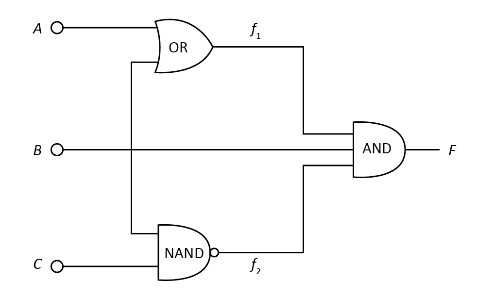
The expression for the f1,f2, is given as,
Now,

Step by step
Solved in 2 steps with 1 images


- SELT-TEST 1. Fill in the blanks by inserting appropriate words/figures. (i) The most common system for secondary distribution is 400..... V. 3-phase. wire system. (ii) In a 3-phase, 4-wire a.c. system, if the loads are balanced, then current in the neutral wire is........ (iii) Distribution transformer links the............ and systems. (iv) The 3-phase. 3-wire a.c. system of distribution is used for......... loads. (v) For combined power and lighting load. system is used. 2. Pick up the correct words/figures from brackets and fill in the blanks. (i) 3-phase. 4-wire a.c. system of distribution is used for load. (balanced, unbalanced) (ii) In a balanced 3-phase. 4-wire a.c. system, the phase sequence is RYB. If the voltage of R phase = 230 20 volts, then for B phase it will be......... (230 2-120 volts, 230 2120 volts) (iii) In a.c. system, additions and subtractions of currents are done (iv) The area of X-section of neutral is generally (r) For purely domestic loads. (vectorially,…a) Explain the construction of LVDT. Identify some suitable examples according to their applications b) Discuss contacting and non-contacting tachometers Note question is taken from instrumentation and measurements courseUsing Kirchoff's law.
- Briefly describe: b) The cause of connection problems when using thermocouples for measurements done remotely (long distance) and its solution.Explain the working of solar poind in briefWhat does the term FACTS mean in the use of power electronics in Smart Networks using appropriate diagrams and giving an example of a typical FACTS controller. Smart Grids use wireless and wired communication techniques – explain the operation of each with the use of appropriate diagrams and the advantages/disadvantages of each.
- A network that is consuming negative reactive power means that it is _____ A. Capacitive B. Inductive C. ResistiveReconsider Problem 3.29. If Va,VbandVc are a negative-sequence set, how would the voltage and current relationships change? (a) If C1 is the complex positive-sequence voltage gain in Problem 3.29 and (b) if C2 is the negative sequence complex voltage gain, express the relationship between C1andC2e) Find the total reactive power in the sound system without using the voltages across loads.Mention the unit. f) Find the apparent power of the system. Mention the unit.