30 k2 I k2 0.201


Q: What are Aυ, Rin, Rout, and the maximum input signal for the amplifier given if RI = 250 kΩ, RS = 68…
A:
Q: Derive the equations for vIN and vOUT. gm1=gm2=1 mS, RX = 75 kΩ, and CX = 1 pF. Ignore channel…
A: Given circuit is as shown below, Given, gm1= gm2= 1mS, Rx = 75 kΩ
Q: Q2: Given VGS(Th) = (4 V) %3D and ID(on) = (4 mA) at VGS(on) = (6 V): 1. Determine k and write the…
A:
Q: Compute the 8-pt DFT of the signal x(n)={*0,0,0,1,3,5} by drawing the corresponding 8-pt FFT…
A: We need to compute the 8-point DFT of the signal x(n)={0,0,0,1,3,5} by drawing the corresponding…
Q: Q3: For the circuit shown find the: Ip, VD, VR, Rp. Draw the characteristic load line curve and find…
A:
Q: Draw the NOR equivalent a) circuit of the expression CD b) c) Draw the NAND equivalent circuit of…
A:
Q: Determine Ip, and Vps, for the enhancement-type MOSFET of Fig. E 12 V Rp 2 k2 RG C2 10 M2 1 µF D…
A:
Q: for the system shown ,Find T.F. Y/X=G(s) by using: a: block diagram technique ? b: signal flow graph…
A:
Q: Shockley's equation defines the. characteristics of the FET and are unaffected by the network in…
A:
Q: Illustrate homomorphic filtering and give its function
A: Homomorphic filtering- The homomorphic filtering is a general technique that is used for image…
Q: For the BJT circuit shown below, determine the value of Ic Vcc. VCE, and R1. Show the details of…
A:
Q: Which value of signal to noise ratio (SNR) is required for attaining the maximum data rate supported…
A: According to the question, which value of signal to noise ratio (SNR) is required for attaining the…
Q: (a) What are the voltages at the nodes in the passtransistornetworks in Fig. For NMOS transistors,…
A: (a)
Q: The circuit shown represents a two-portmodel for a current amplifier. Write expressionsfor input…
A: Given circuit is, Applying the current divider rule at the input side, Applying the same current…
Q: D) Which among the following is a unique model of a system? a) Transfer function b) State variable…
A: Correct option is a) Transfer Function Transfer function is unique for any system wherever coming…
Q: A PSK is used to transmit a digital data with levels {-20v, 0, 10v, 30v), and modulator sensitivity…
A: There are 4 levels in given signals 4 levels transmit if used 2 bits Given,
Q: For the fixed-bias configuration a. Sketch the transfer characteristics of the device. b.…
A: The required parameters can be calculated by using the DC analysis of JFET amplifier circuit.
Q: What is the throughput of a system that use Pure ALOHA protocol to transmit O bit frame on shared…
A: The solution can be achieved as follows.
Q: (a) Consider the minterm function F(A, B, C) = Em(1,3,4,7) ITM Implement the circuit using 4-to-1…
A:
Q: 1. From the obtained data, sketch the transfer characteristics of the JFET. 2. Determine the values…
A:
Q: a. Quantitatively explain about a bridge which is used for the measurement of the High Quality…
A: As per policy i will answer 1st question only. 1.Explain about the bridge which is used for…
Q: Using universitily of NANDs and NORs simplify this equation. ('P+T)(L+'H) + L'H+ P'T
A: Given:-P¯+TL+H¯+LH¯+PT¯
Q: Implement the function F with the following two-level forms: NAND-AND, AND -NOR, OR- NAND, and…
A: Draw the K-map for the above function.
Q: Sketch the transfer curve for p-channel JFET with IDSS 18 mA and Vp -9 V %3D %3!
A: In this question we will draw transfer characteristics for p- channel JFET.
Q: (a) Given VagTh) = 4 V and Ixon) = 4 mA at Vason) = 6 V, determine k and write the gen- eral…
A: a). Determining the value of k, Writing the general expression for drain current,
Q: Q2: Given VGS(Th) = (4 V) %D and ID(on) = (4 mA) at VGS(on) = (6 V): 1. Determine k and write the…
A: According to question we have to, 1. Determine k and write the general expression for ID. 2.…
Q: (b) In a junction of road installed with traffic light, the sensor circuit with capablities to…
A: Given: In a junction of a road installed with a traffic light, the sensor circuit with capabilities…
Q: Using methods discussed in class, please, show all the steps and explain the method used to compute…
A:
Q: G B ? B (a) (b)
A: Whenever we will shift the game block after the summer then we must give the input to the summer…
Q: Ex:-Design NAND gate by using H.As on ly:-
A:
Q: Using approximate method, the DC operating parameters of the common cnitter BIT amplifier are as…
A:
Q: (a) Given VGSTH) = 4 V and Ipxon) = 4 mA at Vas(on) = 6 V, determine k and write the gen- eral…
A: (a) Given values are =
Q: Find the BW efficiency for a wireless communication system having a bit rate of 9.6 Kbps and B Eb of…
A: Given: Bit rate, Rb=9.6 Kbps Bandwidth, B=200 KHz EbN0=10 dB
Q: Q3. Consider a (3,1,3) convolutional encoder with the partially completed state diagram shown in
A: u1=m0⊕m1⊕m2u2=m0
Q: Sketch the transfer characteristics of the device. b. Superimpose the network equation on the same…
A: VDSQ = VDD - ID RD =14 – 4.7*1.8 = 5.54V
Q: Choose the properties which are very important in case of LTI signals and systems? Linearity and…
A:
Q: Hw: Design the following circuit using Decoder F2 = |(0,6,7,8,11,13,14,15) %3D
A: Decoder: A decoder is a rationale circuit that changes over a N-bit two fold info code into M yield…
Q: For the source coding What is/are the benefit(s) of calculating entropy?
A: The entropy of a source is a measure of the average amount of information per source symbol in a…
Q: By using BPSK modulation from a communication channel, voice transmission is made at a data rate of…
A:
Q: Design the following circuit using a Decoder F2 = | |(0,6,7,8,11,13,14,15) П
A: A booelan function can be either expressed in terms of only minterms or only maxterms. Minterms are…
Q: Q1/A/ Ten voice channels each of bandwidth (B.W.)= 3.2KHz are sequentially sampled at 8KHz and…
A:
Q: Using 1st approximation what is the value of ID and VD.?
A:
Q: (a) Given VagTh) = 4 V and Ipxon) = 4 mA at Vason) = 6 V, determine k and write the gen- eral…
A: a). Determining the value of k, Determining the general expression for drain current,
Q: Q3: For the circuit shown find the: ID, VD, VR, RD. Draw the characteristic load line curve and find…
A:
Q: A=101, B=110 ,C= 011, Y=(A NAND B) NOT C = *
A: A= 101 B=110 and C= 011 Find the A NAND B) NOT C This is nand and not operation
Q: The mosfet has the parameters: VTH=0.4, k=200µA/V², and 2=0.001V1, Find: (a) VIN and VDS,Q (b) the…
A: The circuit is as shown below,
Q: Determine p-channel JFET circuit as the Q-point for the shown. Also, plot and properly label the…
A: It is given that:
Q: 14.3.1 - What external circuitry needs to be connected to an 12C bus due to the nature of its…
A: NMOS transistors needs to be connected to I2C bus due to it's open drain transmitter architecture .…
Q: 15. Which of the following leads to the 3G evolution of GSM, IS-136 and PDC systems? a) GPRS b)…
A: In this case, from the given options, the system which leads to the 3G evolution of GSM, IS-136 and…
Use SPICE transfer function analysis to find the
g-parameters for the circuit in as shown.

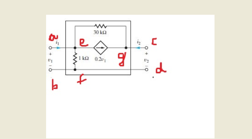
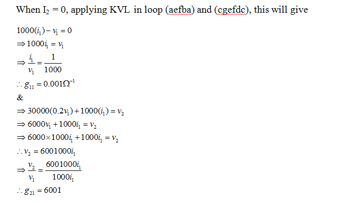

Step by step
Solved in 5 steps with 5 images


